


One topic that has been under hot debate in the semiconductor advanced packaging sector for the past few years is fan-out panel-level packaging (FOPLP). In theory, the concept of taking fan-out from a 300-mm reconstituted wafer to a large panel format as a way to lower costs seems simple, and even the logical step. It’s not.
Skeptics, many burned by the same low-cost advantage argument for investing in 450mm wafer-level technology, poked as many holes in the theory as they could:
- There’s no infrastructure in place to handle panel-level packaging processes
- Where are the tools going to come from?
- Even if we can do it, there’s not enough volume to justify it.
- There are no standard panel sizes
- It can’t be used for high-density fan-out technologies
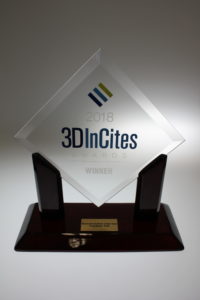
The list went on. But rather than throw in the towel, Fraunhofer IZM in Berlin, saw the opportunity in addressing these questions. In November 2016, they launched a 2-year long consortium of Fraunhofer IZM and partners along the value chain including end users, manufacturing houses (OSATs) and suppliers to tackle the main challenges and make PLP a viable option by the time the industry was ready for it. This effort is what won Fraunhofer IZM the 2018 3D InCites Award for Research Institute of the Year. I caught up with Tanja Braun, group leader of the consortium, for an update on its progress, now that the two years are almost up.
The Back Story
As is the case with many consortia, the reason the PLP Consortium was formed was the realization that moving from 300mm round wafers to panels that can range in sizes from 300×300 mm² to 457×610 mm³ or 510×515 mm² up to 600×600 mm and beyond was not something that could be accomplished alone. This required more than simply scaling up. Materials, processes, and equipment needed to be either adapted or developed. The solution was to involve the entire value chain.
Braun explained that entry into the consortia was possible at two levels: Full and supply chain memberships (SCMs), for which the cost and benefits differed greatly. Full members formed the steering committee and received access to all R&D tasks for their fundamental research. SCMs participated in meetings and are involved in research projects using their materials, services and/or equipment to achieve the goals. SCMs, however, have limited visibility to program information.
Addressing the challenges
By the time the 2017 annual meeting rolled around, the consortia had grown to 17 members including:
- Amkor Technology
- ASM Pacific Technology Ltd.
- Austria Technologie & Systemtechnik AG
- Brewer Science, Inc.
- Evatec AG
- Hitachi Chemical Company, Ltd.
- Intel Corporation
- Merck KGaA
- Semsysco GmbH
- Unimicron Technology Corp.
- and
- Ajinomoto Group
- Atotech Deutschland GmbH
- FUJIFILM Electronic Materials U.S.A.
- Mitsui Chemicals Tohcello
- ShinEtsu Chemical
- SUSS MicroTec SE
- Meltex Inc.
Surprising to Braun is the fact that many SCMs also became full members. “We all saw there was nothing that could be developed alone. We needed partners along the supply chain to provide input about different demands.”
In the first year and a half, Braun says the seventeen partners have made good progress. Together, they merged materials, technologies, and processes. They’ve developed material combinations and sorted out lots of the technical details. They discovered that circuit board knowhow could be leveraged to solve some of the challenges, such as the density gap of high-density substrates. One of the outcomes of the consortia that they’ve joined the SEMI initiative in the establishment of a standardization program for details like panel sizes, features, edge exclusion and warpage.“ We set out to address warpage and die shift, which is getting more critical for larger formats,” said Braun. “Activities include finding ways to do dynamic layout adaption to address die shift.” She added that handling is also an issue as the mold compound is brittle.

What about the volumes?
A funny thing happened since the consortium first formed: fan-out became a big hit. Low-density fan out technologies – the kind that will benefit most from PLP. With mobile chipsets beyond just the processor and modem, including power management ICs, CODECs, and RF ICs, as well as automotive applications, enough volumes will be needed to justify the transition to PLP.
According to Laura Mauer, CTO, Veeco, the equipment company has been recently fielding requests for customers interested in doing panel demos. Previously part of Georgia Tech’s Packaging Research Center’s consortium on both glass and panel technologies, the company had dropped out for a while due to lack of customer interest. “We’ve always had the panel capability for glass panels,” explained Mauer. “Our first 450mm tool developed for wafers had its origins in flat panel displays.” As a result of these requests, the company is interested in joining the next phase of Fraunhofer’s PLP Consortium.
When will PLP be commercialized?
According to Braun, commercialization of PLP is underway. Nepes has already begun running its PLP line with a fingerprint sensor as first application and Deca, Powertech, and Samsung announced it will ramp PLP production in 2018 or 2019. While the early stages of PLP will be in low-density fan-out, Braun sees opportunity in high-capacity for larger package sizes with integrated passives, antennas – other components that require more space and will increase the size of the package.
What’s next?
As the original consortium comes to a close in January, Braun says discussions are underway to extend it, and the interest among existing members is high. After all, there is still work to do. Brittleness, a critical yield-loss issue, still needs to be solved. Additionally, there are lots of questions about fine-line structuring and how to decrease via sizes to achieve 2µm l/s. Additionally. there is still lots of optimization needed for layer-to-layer registration accuracy, multi-layer, and double-sided processing. Companies who are interested in participating in a second PLP consortium should contact Tanja Braun. ~ FvT


