


Once considered to be one of the simpler tasks in semiconductor device manufacturing, IC package design has become more complicated as it becomes more critical to the performance of the end-devices. Market drivers are more varied than ever. Time-to-market is more critical than ever. And advanced packaging options are more numerous than ever. In this exclusive interview with Keith Felton of Mentor, a Siemens Company, winner of the 2018 3D InCites EDA Supplier of the Year, we explore how IC package design has changed over the past decade, and why getting it right the first time is more critical than ever.
With more than 25 years in electronic design automation (EDA) under his belt, Felton can speak historically about package design. He says that over the past 10 years, he can identify three important trends that have had a significant impact on package design approaches. The first is design for manufacture using verification, validation and sign off. The second is the use of digital prototyping to determine the best packaging architecture. The third trend loops back to the first two: and that is the increasing complexity of a package’s physical design.
Verification, Validation, and Sign-off
Gone are the days when package design was as simple as connecting the dots. An IC designer would design a single SoC for a single function, create a routing map for the bumps, and pass it all to the outsourced semiconductor and test (OSAT) service provider, along with a set of specifications for performance, power and cost requirements. It was up to the package team to select the best way to match the bumps with the balls and select the right package configuration to meet the specifications.
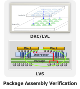
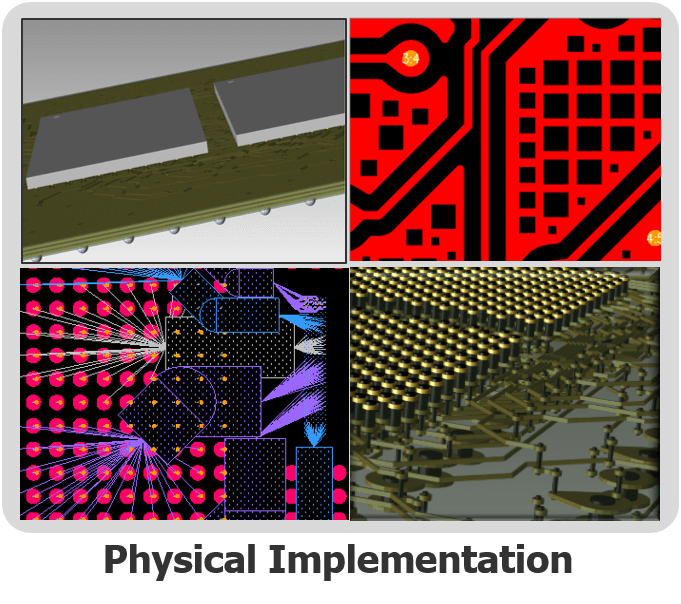
This has changed as packages become more complex due to more connections, routes and increasing high-speed signal content, explained Felton. The introduction of interposers and 3D ICs brought fine geometry manufacturing that required more verification and validation. This complicated the process, requiring more back and forth between the OSAT and the fabless or foundry design team with engineering change orders (ECOs). This resulted in added cost, and delayed time to market. “We started seeing more time spent on package validation,” said Felton. “That’s where people tend to start. Next is how to move the back-end process further forward and eradicate problems early, commonly known as left-shift.” As a result, Felton says Mentor has seen an increased demand for verification, validation and sign-off tools to improve the mask quality of 3D packages to improve yield and performance (Figure 1).
Digital Prototyping
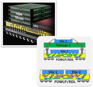
With the explosion of heterogeneous multi-die packages comes multiple sources of design data from different and varied suppliers that must be integrated and work together (Figure 2). Additionally, as IC designers understand and accept that the package is a functional part of the IC versus just a connector for plugging the die into the system, they are taking ownership of package design.
“With 3D packaging, you have two or more disparate die, such as logic, memory, sensors, and even discrete components, all engaged in unique interactions that stay within the package,” said Felton. “In this way, the package becomes an active element. More and more, the IC team is responsible for coming up with the methodology and process that ensures success.”
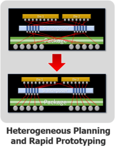
The best way to do this is to begin by gathering all the data and generate digital prototypes to figure out the best way to package the devices to suit any number of scenarios to meet design, cost, and yield requirements. “Some call it co-design, others call it pathfinding. But it’s really (digital) prototyping before committing to a particular package and design,” explained Felton. Essentially, digital prototypes provide models for running different scenarios to determine the impact of different materials, for example (Figure 3)
Designing Today’s Complex Package
Historically akin to circuit board design, new concerns like achieving 2µm line/space, and multiple redistribution layers (RDL) that require high-quality masks, are pushing package design techniques and methodologies into the world of chip design. This is causing package designers to struggle with the overall size and complexity of the designs. In the past, substrate fabrication Gerber data used to be generated in metric minutes. Now, substrate masks must be created as GDSII which can takes hours and must be validated, noted Felton.
As a result, foundries and OSATs alike are tearing a page out of the IC designers’ handbook by providing more comprehensive data in the form of design rule manuals, or as Mentor calls them, assembly design kits (ADKs). “Similar to what happens in the silicon chip world, if I’m designing a 7nm SoC, I will get a comprehensive process design kit (PDK) so that if I design to that set of criteria, I can be confident that my finished design will be manufacturable. Traditionally, that didn’t exist,” said Felton. Rather, a few rules of thumb were provided to design a package. That doesn’t work with 2D enhanced and 3D packaging, he said. Foundries and OSATS were spending so much time revising designs, that schedules are missed and package costs increase.
“The only way to get around the problem is to work with the entire supply change to gather as much digital data as possible about the design process,” he said.
New Package Designs Call for New Tools
From wire bond to flip chip, and even to early generations of stacked die, it was possible to just evolve tools to design the next package type. That’s because the substrate was organic and the technology was similar to a printed circuit board (PCB). Now the packaging world is faced with a dilemma similar to the IC world.

“With the 20nm process came 20nm design tools. We can’t assume the flow and tools developed for 20nm will work for 14nm or 7nm,” explained Felton. “The physics and chemistry evolve at each node change, and that’s starting to happen in the packaging world. We can’t approach new package designs with the same-old-same-old. We have to have new approaches and new tools.”
For example, in fan-out wafer level packaging, (FOWLP) which is a rapidly expanding market, the greatest design challenge is achieving clean foundry/OSAT sign-off. Getting clean mask data using traditional package methodologies and tools that meet foundry requirements has become a struggle. Mask verification for FOWLP and the associated tools is a new area with which package designers need to become familiar, noted Felton.
End Market Impact
Over the past few years, the semiconductor industry has become more and more application-driven, rather than technology driven. As the application window broadens, package design will continue to become more complicated to accommodate the varied requirements.
“Autonomous vehicles, for example, require massive amounts of computing power to process the sensor data in real time – more quickly than the human brain – to respond in time. In those cases, package performance is critically important,” said Felton. “However, IoT wearables have to be functional, yet cost-conscious.”
There are so many variables to consider depending on the target market application. This is another great reason why digital prototyping is so important. Getting package design right the first time means balancing cost, size, performance, and package type. It all depends on what needs to be achieved.
To learn more about Mentor’s approach to ADKs, check out the Mentor white paper series on the 3D InCites Knowledge portal. ~ FvT


