


Part 2 of the series, The Triumph of Quantum Mechanics at the Heart of Solid-State Data Storage, continues with a history lesson on the invention of tunneling-based flash memory.
In 1956, William Shockley, shared the Nobel Prize in physics with J. Bardeen and W.H. Brattain, all at Bell Laboratories, “for their researches on semiconductors and their discovery of the transistor effect”. The prize was based on their 1940’s work on the point contact transistor that evolved into the junction bipolar transistor. The more important (from a practical point of view) field effect transistor had not yet been made.
In his Nobel Prize Lecture, Shockley stated: “it seems highly probable that once the phenomena of surface states are thoroughly understood from a scientific point of view, many useful suggestions will arise as to how this knowledge may be employed to make better devices”. This stands out as a massive understatement given the fact that the silicon microelectronic revolution is built on the invention of the field effect transistor that depended on the control and passivation of surface states.
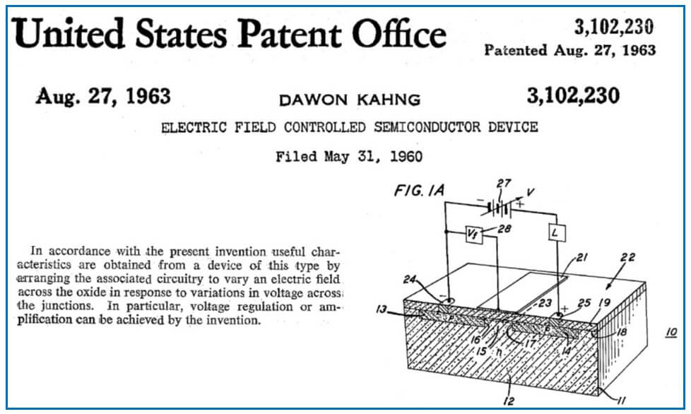
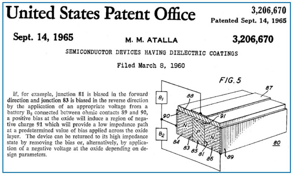
At the end of the 1950’s, Bell Laboratories in New Jersey had already established itself as the center for semiconductor research and development. Practical implementations of the field effect transistor, originally invented by J.E. Lilienfeld in 1925 and O. Heil in 1934, had been elusive until it was found that oxidation of a silicon surface resulted in a silicon dioxide (glass) layer that was stable, had a high dielectric strength and passivated the silicon surface by removing the effects of charged surface states. This then allowed an external transverse (perpendicular to the surface) electric field to modify the electrical conduction properties close to the silicon surface. Figures 8 and 9 show excerpts from D. Kahng and M.M. Atalla’s silicon field effect transistor patents. Both worked at Bell Laboratories.
The invention of the silicon field effect transistor in 1960 started a race to develop integrated circuits and new types of devices that could be used as semiconductor memory.
The first nonvolatile (retaining their memory state without external power) memories based on charge storage within the field effect transistor started to make their appearance in 1967.
The general memory concept involves storing charge between the gate electrode (“87” in Figure 9) and the surface channel (“91” in Figure 9). This stored charge changes the “threshold voltage” of the transistor, defined as the gate electrode voltage (with respect to the source electrode — “86” in Figure 9) at which appreciable current starts to flow in the channel between source and drain (between “86” and “84” in Figure 9).
The silicon field effect transistor acts as an electrometer to measure the stored charge.
Two main nonvolatile memory concepts arose at about the same time across several laboratories:
- Storage of charge in a thin film of silicon nitride between gate and channel.
- Storage of charge in a “floating gate” between gate and channel.
Figure 10 shows the first report, in 1967, of the silicon nitride approach that became known as (metal-gate, silicon nitride, silicon dioxide, silicon (MNOS). Charge tunneled through the silicon dioxide layer into and out of “traps” in the silicon nitride layer. The presence or absence of this charge was read out by determining the threshold voltage of the field effect transistor.
Figure 11 shows a variation of the silicon nitride approach called metal-gate, silicon dioxide, silicon nitride, silicon dioxide, silicon (MONOS) that was reported in 1968. Note the statement “This phenomenon has been explained as electron tunneling from the semiconductor through the oxide into the traps in the nitride”.
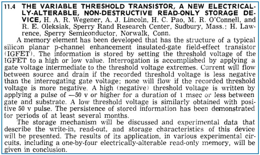
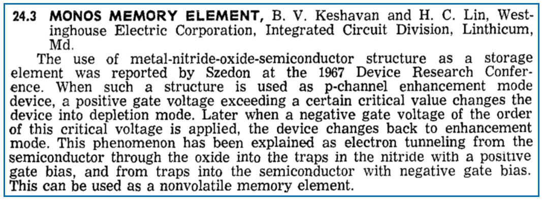
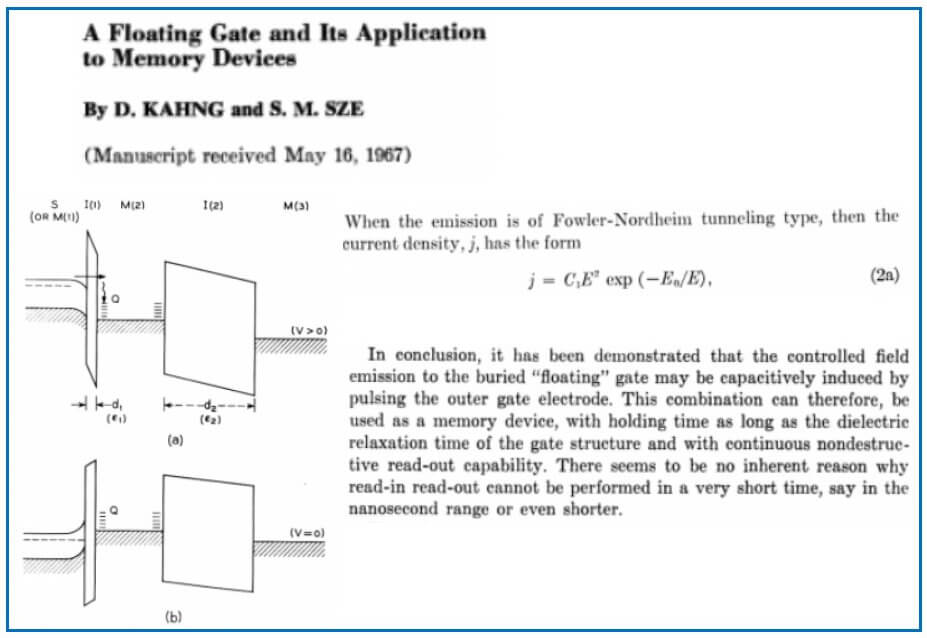
Figure 12 shows the first report, in 1967, of the floating gate approach. Note the energy band diagrams showing (from left to right) the silicon (n-type), a thin silicon dioxide tunneling layer, a floating conductor, a thicker dielectric layer and a metal gate electrode. Note also the explicit use of the Fowler-Nordheim tunneling equation. Interestingly, the arrow in the Figure showing the tunneling of electrons is strictly speaking direct tunneling and not Fowler-Nordheim.
Fairchild Semiconductor, set up by the “Traitorous Eight” who had problems working with William Shockley, had started work on the “MOS” (Metal-silicon diOxide-Semiconductor) system in 1963. This included extensive work on the physics of tunneling in the two silicon nonvolatile memory concepts between 1967 and 1969.

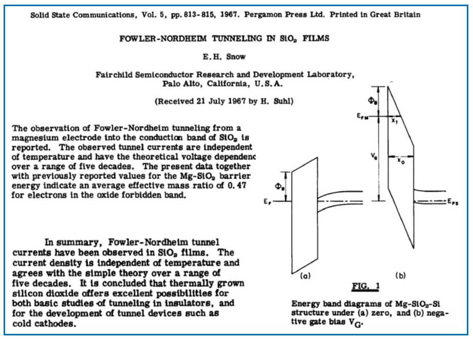
Edward Snow at Fairchild published a paper in Solid State Communications in October 1967 (received July 1967). Figure 13 shows excerpts from his “Fowler-Nordheim Tunneling in SiO2 Films”.
In about 1967, Martin Lenzlinger joined Fairchild reporting to Edward Snow in the surface physics group. Figure 14 shows excerpts from Lenzlinger’s laboratory notebook in late 1967.
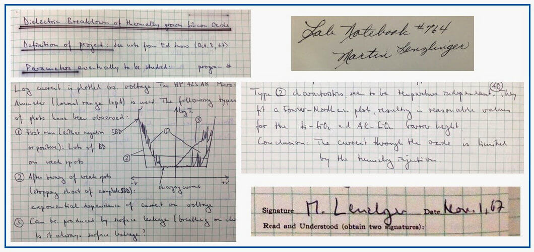
Figure 14: Excerpts from Martin Lenzlinger’s laboratory notebook at Fairchild in late 1967. Fairchild Semiconductor notebooks and technical papers, Box 36, Catalog #102722994. Reproduced with the permission of Computer History Museum (Shustek Center, Fremont, California).
Lenzlinger was studying the conduction properties and breakdown in thermally grown silicon dioxide. After “burning” away weak spots in the oxide (in a fuse-like manner), he managed to reproduce the Fowler-Nordheim tunneling conduction that Snow had achieved with magnesium as the capacitor metal electrode and extended it to aluminum as the electrode.
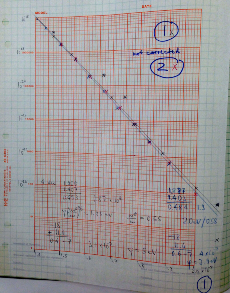
Figure 15 shows the “Fowler-Nordheim plot” from Lenzlinger’s laboratory notebook of December 1967 where the y-axis is the logarithm of the (current density divided by the square of the electric field) and the x-axis is the inverse of the electric field.
Lenzlinger’s work resulted in two papers appearing in 1969 in the Journal of Applied Physics.
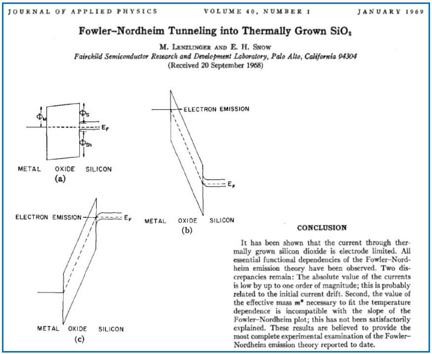
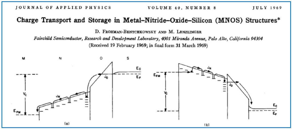
Figure 16 is the “Lenzlinger and Snow” paper describing Fowler-Nordheim tunneling in thermally grown silicon dioxide. Figure 17 is the “Frohman-Bentchkowsky and Lenzlinger” paper describing electron tunneling into and out of a silicon nitride storage layer. The conduction through the silicon dioxide layer is Fowler-Nordheim tunneling.
These fundamental studies in the late 1960’s, focusing on the two types of charge storage in a MOSFET (Metal-Oxide-Semiconductor-Field-Effect-Transistor), silicon nitride-based and floating conductor-based, set the scene for a proliferation of further work and the first silicon integrated circuit nonvolatile memory products within the next decade and laid the foundation for the rise of NAND Flash and the solid state data storage revolution. ~ Andy Walker
Read part one in this series here.
Header image: M. Lenzlinger laboratory notebook, p.6, Dec.12, 1967 (#764), 1967–1970, Fairchild Semiconductor notebooks and technical papers, Box 36, Catalog #102722994. Reproduced with the permission of Computer History Museum (Shustek Center, Fremont, California


