
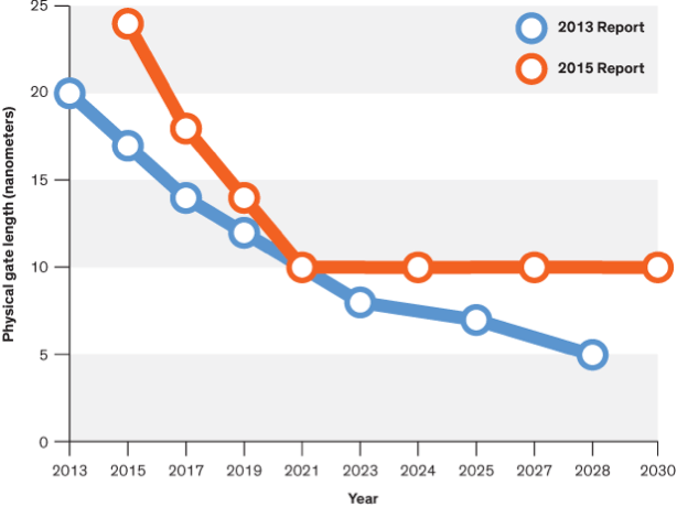
There is fierce competition for scaling foundry logic technologies. However, according to the 2015 International Roadmap for Semiconductors (ITRS), logic transistor scaling will stop at 10nm and it will no longer be economically desirable for companies to continue traditional transistor miniaturization in microprocessors1. How will this impact the lifespan of CMOS integrated circuits? (Figure 1)
In the case of memory devices, DRAM and NAND faced scaling limitations at 18nm and 14nm, respectively. However, we don’t feel these scaling limitations at this moment because many products are still using old generation technologies and gradually moving to advanced technology nodes with tool upgrades. So, memory devices are still achieving 25% to 35% bit growth every year. However, such bit growth will end in few years. Then, what will happen? The lifespan of CMOS integrated circuits will end.
At the transistor level, FD-SOI, later nanowire, and vertical nanowires are being developed as a replacement for FinFET. However, regardless of the technical feasibility of these technologies, transistor scaling will not be meaningful under 10nm technology node if manufacturing costs cannot justify the cost of production.
Therefore, instead of lateral scaling the transistor, vertical scaling seems an inevitable choice for the semiconductor industry.
However, 3D IC logic technology, which implements a logic IC on top of another logic IC is extremely difficult2, considering the optimization of at least 15 to 20 different transistors at low temperature, because each of these transistors needs different gate oxide, channel doping, annealing for damage cure, dopant activation, junction depth optimization, leakage current optimization, well dopant formation, and breakdown voltage optimization through multiple high-temperature heat cycles. In addition, economically, there is no strong reason to implement 3D IC logic because overall yield will drastically drop as the number of layers increases. If there is no disruptive idea to reduce the cost of 3D IC logic, folding 2D logic IC to implement 3D logic IC does not provide cost reduction.
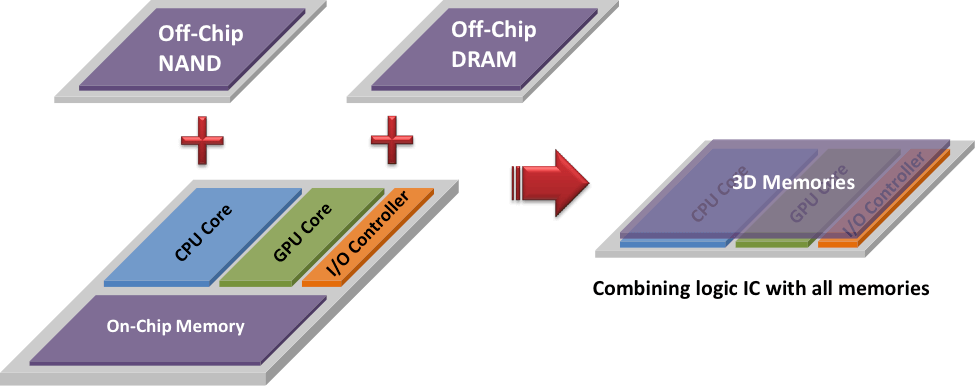
Instead of chip-level 3D IC logic integration, we should consider system-level 3D IC integration in order to find low cost and high-performance solutions. Here is and example of system-level, especially memory sub-system level, integration of 3D IC that combines logic IC with on-chip and off-chip memories. It implements memory cells on top of logic IC. Unlike logic IC which needs 15 to 20 different transistors, only one transistor type is needed for a memory cell. So, it is technically feasible to optimize the single transistor at low temperature.
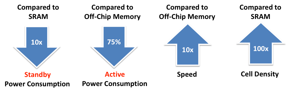
On-chip 3D memories could significantly boost the performance of logic products because on-chip memory is about 10x faster than off-chip memory. Also, it could reduce power consumption up to 75% in the memory sub-system because no I/O is needed between CPU and off-chip memory.
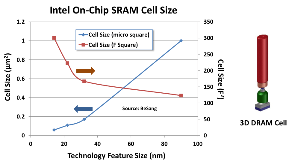
The graph in figure 3 shows Intel’s on-chip SRAM cell size. SRAM used to be 100F2 at 100nm feature size. It now becomes more than 300F2 at 14nm feature size. This means SRAM becomes inefficient. At 22nm node, 3D DRAM could install 100 times more memory cells compared to SRAM. In addition, standby power consumption of 3D DRAM is about 10x less than that of SRAM.

Summary
It is clear that lateral transistor scaling faces its limitation. So, vertical scaling is the only option for the semiconductor industry. For a long time, the semiconductor industry has searched for a solution for vertical scaling. Unfortunately, there is no major progress yet. In the case of memory, 3D NAND successfully started mass production. However, we don’t see cost advantage from 3D NAND yet3. No one knows when 3D NAND will achieve price parity with planar NAND. In the case of logic, it seems extremely difficult to implement 3D IC logic at low temperatures. In addition, cost reduction must be an important challenge for 3D IC logic.
So, instead of chip-level 3D IC integration, we should consider system-level, especially memory sub-system level, 3D IC integration in order to find out low cost and high-performance solutions. It will create huge value for logic products. 10x reduction in standby power consumption compared to SRAM, 75% reduction of active power consumption from memory sub-system, 10x fast access time compared to off-chip memory, and 100x more cell densities compared to SRAM. So, system-level 3D IC integration of logic IC with memory will defy the scaling limitation of logic products and expand the lifespan of CMOS integrated circuits.
References
- Rachel Courtland, “Transistor Could Stop Shrinking in 2021” IEEE Spectrum, Jul. 2016
- Hae-Young Lee, “New Semiconductor Exceed Moore’s Law Limits?” Associated Press, Sep. 19, 2016
- Colin Johnson, “3D NAND Flash at 2 Cents per GB,” EE Times, Jul. 18, 2016


