

Part 1 of my 3D ASIP blog covered the five keynotes presented at 3D ASIP 2017. Part 2 focuses on more than 20 informative presentations, where focused experts gave an in-depth view of new and/or improved technologies for 3DIC-related advanced packaging. Before we address these, allow me a one-sentence recap of Part 1’s key message:
We no longer have one major application, like mainframes, PCs, and smartphones, driving the progress of primarily digital SoCs; but rather face a diverse spectrum of lower volume opportunities that often require a combination of heterogeneous functions. Significant changes are needed to keep/accelerate our industry’s growth, like utilizing higher-density IC packaging for heterogeneous integration, because it’s the most promising approach for system scaling in the foreseeable future.
The individual experts’ messages started on Tuesday afternoon with several presentations from equipment and materials suppliers.
Tom Strothmann presented challenges Kulicke & Soffa (K&S) faces when developing the equipment for manufacturing 3DICs in high volume, specifically Hybrid Memory Cubes (HMCs) on substrates and High Bandwidth Memories (HBMs) on wafers. He explained how K&S meets productivity and accuracy goals for thermal compression bonding of multiple memory dies, interconnected with copper studs and through silicon vias (TSVs). To maximize thermal conductivity between the dies, K&S uses either capillary underfill (CUF) or non-conductive film (NCF).
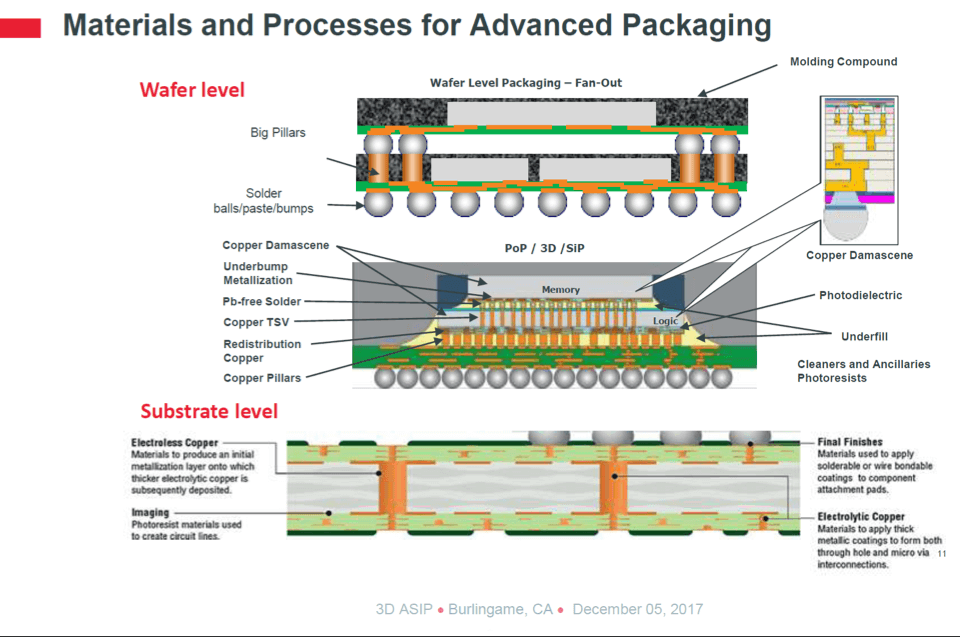
Rozalia Beica explained how the recently merged chemical giants Dow and DuPont address the materials requirements for advanced IC packaging. Figure 1 shows examples where materials play very important roles in streamlining manufacturing and assuring performance and reliability of single and multi-die ICs.
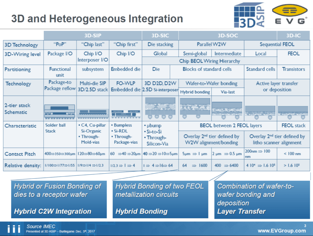
EV Group’s Thomas Uhrmann presented equipment and process solutions for a broad range of integration alternatives and positioned EVG’s manufacturing solutions accordingly. Uhrmann used the matrix imec presented at last year’s 3D ASIP conference to do so. Figure 4 shows how EVG equipment and processes capabilities address all these integration alternatives.
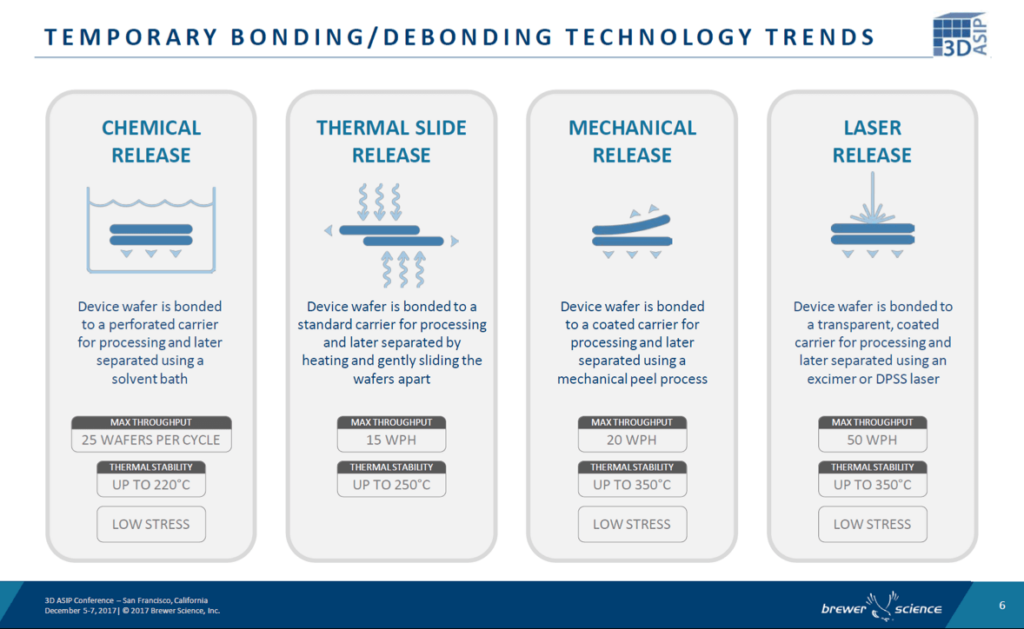
Kim Yess from Brewer Science showed a very clear overview of temporary bonding/debonding steps, discussed these alternatives and highlighted their specific challenges (Figure 3). She also talked about the evolution in substrate buildup and explained the need for developing new materials for advanced wafer and panel-level packaging.
The next speaker, Javier DeLa Cruz’ from Invensas, a subsidiary of Xperi, described in his presentation how image sensors, memory stacks and other 3DICs that need fine-grain interconnects between dies, benefit from the much tighter (< 1 mm) contact spacing Direct Bonding Interconnect (DBI) technology enables. Compared to Cu studs (which allow only spacing in 10s of microns), DBI also offers excellent thermal conductivity between the dies, without the cost or manufacturing challenges of adding underfill.
The next session focused on how and where 2.5/3D-IC serve specific applications much better than single-die SoCs.
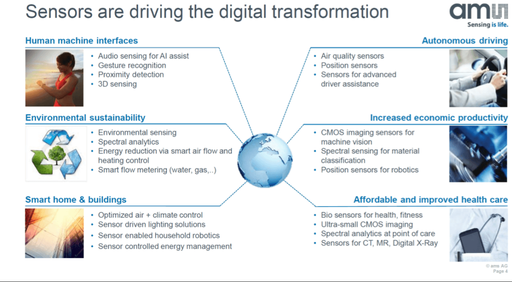
Franz Schrank from amsAG in Austria showed examples how ams’ developers serve sensor applications with their own 2.5/3D platform solutions. He explained the essential role sensors play in the transformation of analog signals around us to digital data, suitable for processing. He categorized ams’ target markets as shown in Figure 4.
While Schrank included a lot of application-specific topics and customer perspectives in his message, the next presenter, Krishnamoorthy Balachandran from Cisco brought a true customer perspective to the conference. As he talked about HBM test challenges, it became clear that there is a price to pay for being one of the first beneficiaries of the significant benefits this memory subsystem brings to high-performance interposer designs. There is clearly a lot to learn when deploying HBMs in volume production. He asked for better user education and cooperation across the ecosystem from design to manufacturing, and, of course, wants all contributors to emphasize testability.
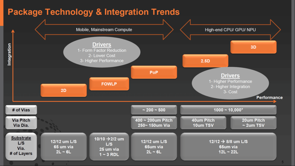
Hamid Eslampour gave an overview of GlobalFoundries capabilities and explained their business model for developing 2.5D and 3DIC designs for and with customers. He emphasized that GlobalFoundries takes responsibility for an entire customer project, even if it’s jointly executed with assembly and test partners. Figure 5 shows how GlobalFoundries uses advanced packaging technologies to enable system scaling and with it, improve performance per Watt, form factor and system cost. Eslampour also mentioned their proven cooperation with AMD to develop and manufacture multi-die ICs, like the EPYC processor introduced in June 2017. Lisa Su, AMD’s CEO presented at IEDM 2017 some of the important benefits her team reaps from multi-die packaging. See key benefits described in my recent IEDM blog.
Gamal Refai-Ahmed presented for Xilinx. In 2011, they combined four FPGA dies on an interposer and introduced the first multi-die IC, the Virtex 7 2000T. LUT-count and performance per Watt exceeded the FPGA competitors’ solutions by far and allowed emulation of much larger circuits, faster and at a magnitude lower power than available from others. Knowing the benefits of multi-die integration in a single IC package well, Xilinx has developed a family of interposer-based FPGAs and integrated heterogeneous functions. When asking for a stronger ecosystem around multi-die integration, Refai-Ahmed explained the important role of the Heterogeneous Integration Roadmap (HIR) team and invited conference attendees to contribute to it.
Sergey Shumarayev brought Intel’s multi-die perspective to this session. He talked about Intel’s Embedded Interconnect Technology (EMIB) technology and it’s role for high-speed computing to, above all, significantly improve performance per Watt. He mentioned that Intel’s Nervana neural network processor IC is a multi-die solution, using EMIB, to interconnect logic and memory dies (HBMs).
In addition to Dan Green’s DARPA keynote, see part 1 of my blog, (pointer, please) several more Military / Aerospace-focused presentations followed his visionary keynote.
Pavel Borodulin from Northrop Grumman endorsed DARPA’s call for chiplets and a user-friendly methodology to combine them on interposers. He highlighted a large number of I/Os needed on individual ICs for printed circuit board (PCB) mounting. Also, the I/Os power dissipation and the energy (picojoules per bit) it takes to transmit signals between ICs on a PCB, is a big challenge. These and the significantly smaller form factor interposer-based designs enabled are Northrop’s key motivators for contributing to DARPA’s CHIPS program.
Zhengya Zhang, from the University of Michigan, outlined his efforts in developing flexible and programmable I/Os in support of DARPA’s CHIPS program. He also discussed how programmable neural networking principles should be applied to interposer designs.
Lockheed Martin’s Rick Stevens presented why and how the modularity of interposer-based designs will simplify redesigns and re-qualifications without changes to a board and/or system; especially the very long product lifetimes of military programs required to replace end-of-life components quickly and cost-effectively. Compared to current ICs, the modularity of interposer-designs enables redesigning only the obsolete portion of a heterogeneous multi-die IC, which is easier than redesigning entire ASICs or SoCs.
Tim Lee, a fellow at Boeing, gave an overview of their Hi-MIPS program, ongoing with DARPA. Lee amplified the importance of replacing obsolete parts with a compelling example: The B52 airplanes were introduced in 1952 and will remain in service until 2045. In our fast-paced semiconductor industry, lots of changes to semiconductor components are likely to happen during decades of system lifetimes. Lee also mentioned their cooperation with UCLA’s Chips program and joint efforts with Yuan Xie at UC Santa Barbara.
The next session focused on advanced assembly technologies.
Stefan Behler, Besi, demonstrated the company’s vast expertise in thin-wafer handling and presented many measurement results to substantiate Besi’s strengths.

Koyanagi-san from Tohoku University explained how to use hydrophobic and hydrophilic material characteristics to achieve very quick and highly accurate self-alignment of chiplets with the help of water droplets.
Teledyne’s Andy Carter showed how they use micro-transfer printing to place high-performance InP Heterojunction bipolar transistors on GaAs, Si and SiC substrates.
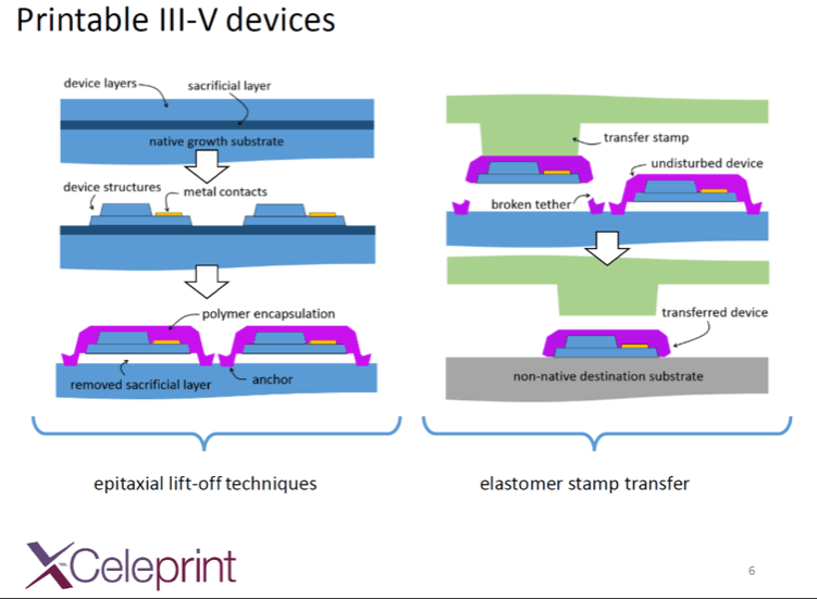
X-Celeprint’s Kanchan Ghosal also focused on microprinting and presented how his company uses epitaxial lift-off techniques and elastomer stamps (see Figure 6) to transfer tiny devices onto larger dies, interposers or substrates. He stated that the displacement error at 3 s is +/- 1.5mm.
Eugene Chow from PARC was the third speaker who focused on micro-printing. It’s clearly an important technology to integrate heterogeneous functions cost-effectively.
The focus of the next session was Fan-out Wafer-level Packaging (FOWLP).
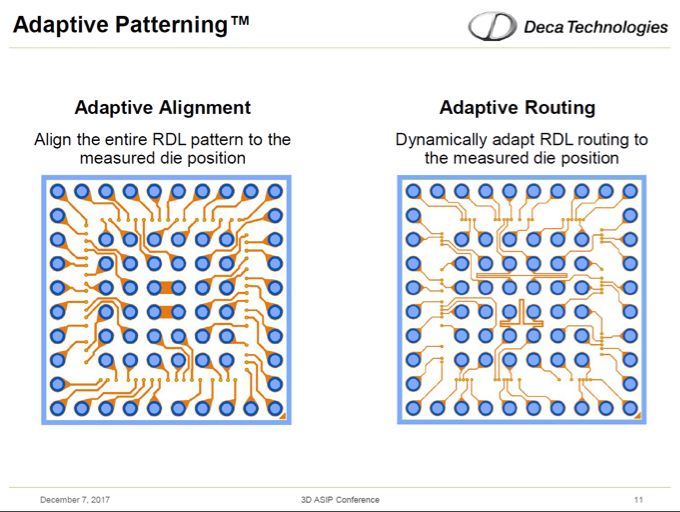
Chris Scanlan from Deca, a Cypress subsidiary, talked about their M-Series packaging technology’s capabilities and highlighted the proven benefits of Adaptive PatterningTM techniques that compensate for die alignment variations and needed routing changes to improve manufacturing yield. See Figure 7 with examples of adaptive placement and routing. This is an especially important technology for the emerging panel-level processing technologies, where accurate alignments are more difficult to achieve than on wafers. FYI: ASE licensed this technology and invested $ 60 M in Deca in 2016.
Amkor’s Ron Huemoeller gave an overview of current capabilities and an outlook of the packaging future. He compared the geometries of different levels of integration:
- PCBs offer >30mm Line/Space and >100 mm vias today
- Substrates allow 10-30 mm L/S and 30-100 mm vias
- What he called “OSAT level” allows 2-15mm L/S and 5-30mm vias with organic materials
- What he called “Foundry level” allows, with silicon interposers, < 1mm L/S and ~ 1-2mm TSVs today
Looking at these numbers, it’s obvious that the level of system integration significantly impacts – in addition to form factor and weight – the performance per Watt and the success of an electronic system. Huemoeller also pointed out that 5G communication and automotive lidar equipment, using up to 80 GHz mmWaves, require low loss RF front-ends and antennas or antenna arrays integrated into the package. For these new materials are needed to minimize insertion loss (a.k.a. loss tangent) of molding compounds, substrates and interposers.
The next speaker was Vinayak Pandey from JCET/STATSChipPAC. His message centered around their embedded wafer-level ball-grid array technology (eWLB), how it’s applied to mmWave applications and that it’s qualified for automotive Grade 1. Pandey also mentioned that the integration of photonics introduces new requirements for IC packaging.
Intel’s Mike Skinner presented, from a patent attorney’s perspective, how important it is to protect your own intellectual property and respect other companies IP and suggested steps to stay out of trouble.
After a short coffee break, the image sensor session started.
SONY’s Hayato Wakabayashi presented several strengths of their very widely used 3DIC image sensors. He explained how they achieve 2360 x 1728 resolution, sensitivity and color accuracy at low cost, He also compared the benefits of global shutter versus a rolling shutter.
Right after SONY, the #1 image sensor supplier, Yoshiaki Takemoto from Olympus presented their strengths. Olympus is the # 3 image sensor supplier, after TSMC.
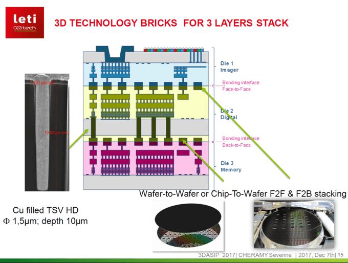
The final presentation of this session was delivered by Leti’s Severine Cheramy. Figure 8 shows how Leti vertically integrates, at the wafer-level, the imager – with 1.4mm pixel pitch – the DSP circuitry, and a memory die. backside illuminated imager and logic are interconnected face-to-face using hybrid bonding, while logic and memory are connected back to face, using TSVs and hybrid bonding. Cheramy mentioned that Leti is evaluating if/how Leti’s CoolCubeTM technology can be utilized for image sensors.
A quick recap of Part 1 of this blog:
3D ASIP 2017 was the 10th edition of this conference I have attended. These ten conferences gave me enough data points for a quick look back in time and for a regression analysis to project the next few years.
Very quick look back: The manufacturing ecosystem has made enormous progress and has selectively engaged with EDA vendors – see a summary of Mentor’s presentation in part 1 – and worked with leading-edge IC and system designers to roll out high-performance computing/graphic/networking solutions, smart-watches, and other wearables.
Looking ahead again, I would say: As soon as the manufacturers, in cooperation with EDA vendors, can develop many more library and IP building blocks (chiplets) and user-friendly die – package – board design methodologies, the number of users will grow rapidly. Sorry, it’s beyond my pay grade to tell you exactly in which year the broad multi-die IC technology adaption wave will be in full swing. ~ Herb


