
There is an active and robust supply chain currently supporting these wafer sizes in the semiconductor manufacturing industry: 3”; 4”; 6”; 200mm; 300mm; and 330mm. This wide range of substrates is successfully being used today for “sweet-spot’ manufacturing of LED, compound semiconductor, MEMS, trailing-edge CMOS, leading-edge CMOS, and fan-out wafer level packaging (FOWLP) applications, among others.
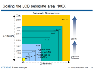 And there is an active and robust supply chain currently supporting various panel sizes in the flat panel display manufacturing industry today, sizes that start somewhere down around “Gen 3” glass panels (550mm x 650mm) and run all the up to “Gen 8” (2200mm x 2500mm) and beyond.
And yet there are strong concerns being loudly voiced at recent advanced packaging conferences and symposiums contending that, because there are a variety of panel sizes being explored for fan-out panel level packaging (FOPLP), a robust production supply chain in the FOPLP industry cannot be established until after a single panel size becomes standard.
I say that by all means, standards are a good and necessary thing: we have standards, from SEMI and others, for 200mm silicon wafers, we have standards for 300mm silicon wafers, and we even have standards for 450mm silicon wafers, ready for when that big day comes.
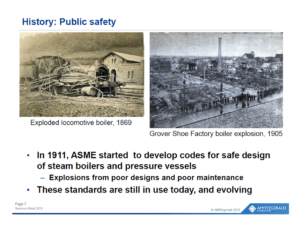 And we are better for it – this framework of standards, that is. (Note for example the terrific work and calls-for-action Dr. Alissa Fitzgerald has been promoting regarding standards for the MEMS industry.)
But you hear no one crying today that semiconductor manufacturing can only be economically rewarding, either for device makers themselves or for the capital equipment suppliers and material suppliers in their supply chain, at a single wafer size.
If anything, the past few years have shown renewed vigor for 200mm silicon manufacturing. And the supply chain responded by building new 200mm equipment of standard design, by supplying refurbished 200mm equipment of established design, and by going out and, yes, putting new engineering effort into upgraded designs for 200mm processing gear.
That made everybody happy.
During my recent trip to Singapore, when I wasn’t talking with cab drivers about solving the problems of the world, I was looking out the window clocking cars. (I’m in the market for a new one.)
And it struck me, looking at cars on the road 8,000 air miles from where I live: There are standards for automobiles, but there is no “standard automobile.”
What cars there are on the road in Singapore, well, that’s up for the customer to decide – the Market Forces, as it were, interacting with automobile suppliers.
By my tally, the single most-represented car in Singapore last week was the Honda Vezel – the small SUV we call the HR-V in California.
The Vezel seems a good car for Singapore, and it seems Singaporeans are responding.

But here in Silicon Valley, the Vezel / HR-V is a bit of a rarer bird. It’s Teslas, or BMWs, or even eGolfs that are popular.
And that’s OK. Because one size doesn’t fit all.
So, just as exists in semiconductor device fabrication and in flat panel display fabrication today, multiple formats, multiple panel sizes, should be OK for the FOPLP industry.
His Vezel may be her Tesla may be my GTI.
In automobiles, that’s SOP, even if it took decades and decades to evolve from the Model T (“Any customer can have a car painted any color that he wants so long as it is black”) days to the peacock age of today.
It’s reasonable to think the FOPLP industry should be the same, thriving on variety, with the supply chain responding gratefully to the Invisible Hand rather than trying to constrain said hand unnaturally.
From Santa Clara, CA, thanks for reading. ~PFW


