The Challenges of Manufacturing 3D Stackable Memory
Memory technologies vying to fulfill the increasing capacity and density requirements of the solid-state storage market two years from now will be confronted by having to meet demanding cell performance and cost-per-bit metrics to be viable. Today, NAND technology is still the primary solution for building solid-state storage devices (SSD), as the once-promising phase-change memory technology has now lost support among the major industry players as a replacement for NAND. But NAND’s future is limited.
From a cell performance standpoint, planar NAND cell technology has hit its scaling limits at the 1Y node. 3D NAND is being considered as the next alternative to planar NAND because of the additional cost reduction and scaling it enables. But cell performance in 3D NAND is poorer than in planar NAND, and this in turn results in increased controller and system complexity and cost. As a result, the potential die size gains that can be realized from stacking NAND cells are limited.
The question then is which technology will step up to replace NAND once the die size gains from stacking current NAND cells plateaus. What’s needed is a fundamental cell that can deliver the greater performance metrics required for next generation memories together with the potential to scale and stack in 3D. Such technology would quickly become the prime candidate to replace NAND in a 3D stacked memory architecture.
Resistive RAM, RRAM, is the only viable alternative to NAND over the next few years because of its advantages in cost, manufacturability and overall system performance, and today many “flavors” of RRAM technology based on various materials are being developed by existing memory industry leaders as well as by emerging companies.
In Part One of this two-part series, we will look at the challenges that need to be overcome in manufacturing 3D stackable memory using the competing technology approaches. In Part Two, we will focus on the advantages inherent in resistive memory technology over current NAND technology in taking 3D memory on a familiar and reasonable cost curve to 8-nm technology nodes.
Challenges in Creating 3D Stackable Memory
Any 3D technology that seeks to replace current planar NAND will have to meet several rigorous requirements, most notably cell performance that is significantly better than current standards and a lower cost per bit than that of current 2D devices, as well as the increased physical demands imposed by stacking.
Cell Performance – Maintaining the status quo or achieving only an incremental improvement in cell performance will quickly outweigh the density improvement achieved with stacking. In other words, while there will be an initial linear improvement by stacking multiple layers of current-technology cells, it cannot be maintained because of two issues. First, cell performance will degrade as more layers are added on top during the manufacturing process, requiring larger, more complex controller circuitry to compensate for this. And so any gains made in array area by stacking will be offset by larger and larger peripheral circuitry. The second issue is yield. Connecting layers by vias that run through the cells has a greater impact on yield than when cells are connected only at the ends for wiring.
Given these two limitations, a memory cell will need to deliver at least a 20X overall improvement in performance metrics. Achieving this will require operating at a lower voltage (preferably <2 V) and with lower power. This means cells with fast switching times and high enough on currents when turning on, the ability to do fast resets and a low enough leakage in the off state to enable arrays that exhibit minimal or no crosstalk between cells. The cells should also be able to be controlled by simple circuitry that does not require significant chip real estate.

Stacking such an array of cells in multiple layers to achieve a 3D architecture also implies the ability of the cells to withstand the impact of additional layers. This is analogous to adding more floors to a building. The lower floors must be able to handle the weight and should be structurally matched to the floors that go on top of them. The basic building block of each floor has to be able to withstand the impact of adding floors above it, irrespective of the other floors above or below it. In the memory architecture, however, it is the mechanical stress, thermal budget and electrical outputs that have to match instead of weight and structure.
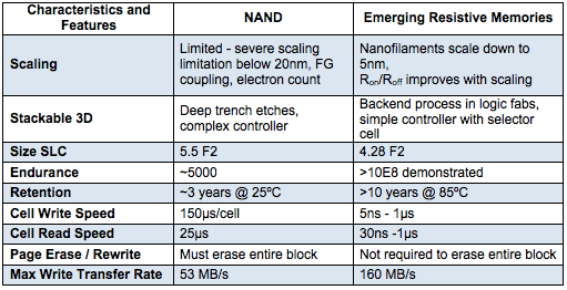
Table 1 compares some of the key cell performance metrics and data currently available for NAND devices and emerging resistive memories.
Cost Per Bit – The primary challenge in reducing the cost-per-bit for a stackable 3D memory is in optimizing the three dimensions of the 3D memory (for a given memory density) with respect to cost.
While stacking more layers might theoretically increase the number of bits for the same die size, in reality, this is bounded by die yield, which affects cost, and the size of the control circuitry, which increases in complexity and takes up more area.
This tradeoff is the reason why more robust cell technologies and different ways of stacking arrays are being explored by the 3D memory industry. Among the approaches being explored are making the memory stack layers and the control circuits on two separate wafers and then bonding them together, using interposer wafers to connect memory wafers to logic circuit wafers, or multiple layers of memory stacked not monolithically but by bonding methods to reduce die size. But all of these approaches have cost limitations due to process complexity and yield.
From a manufacturing perspective, cost per bit is determined mainly by the equipment requirements of the fabrication process and the number of process steps required, and by the yield and time to maturity of the process. Going from the current planar NAND manufacturing to 3D NAND manufacturing has increased fab costs for current memory makers. The tools expenditure and fab upgrades required for existing technology nodes to do 3D memory are likely to be in the billions of dollars. This investment is expected to get NAND on current cost curves for at most five years of production, based on current tear downs of 3D devices and analyst projections.
If RRAM cells are to replace NAND cells, they will have to be manufactured using existing fab equipment, with only a limited number of additional process steps compared to a normal logic process.
Any 3D technology that seeks to replace current planar NAND will have to meet several rigorous requirements, most notably cell performance that is significantly better than current standards and a lower cost per bit than that of current 2D devices, as well as the increased physical demands imposed by stacking. Despite these challenges, there are opportunities for resistive memory cells to take current 3D memory on a cost curve to 8-nm technology nodes with which the industry is familiar.
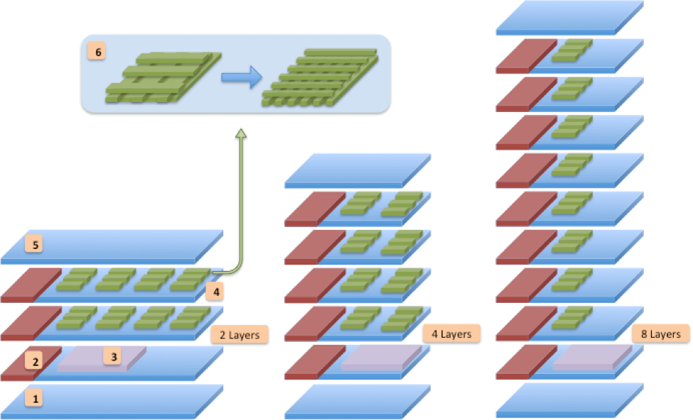
Optimum 3D stacking – 3D chip cost must be optimized in all three dimensions. The x and y axes, which define the chip area, must be optimized for density, as well as in the z axis, which is determined by the number of layers, as shown in Figure 1.

As shown in Figure 1, the same total memory density may be achieved in three ways by using two, four or eight layers of different densities. But each configuration is affected differently by how the fixed area under the memory is allocated. Part of this area is allocated for control circuitry that can be tucked under the memory layers and part is for things that cannot.
In this example, using two layers leaves a lot of the area available under the memory empty and wasted. With four layers, the chip area under the memory can now be reduced and the result is optimized for this memory density. Going to eight layers, however, does not reduce the chip size further. It significantly increases the cost of manufacturing without offering any compensating die size reduction. The effective number of bits in each layer can be increased by going to denser metal lines, but this has an adverse impact on the controller area.
The optimal solution is achieved by understanding the roles of and balancing the following four factors:
- The area of the controller that can fit under the memory layers,
- The area overhead that cannot fit under the memory layers (array efficiency),
- The number of bits in each block relative to factors 1 and 2 above, and the optimized layering for a given density.
Part Two will discuss the attributes of resistive memory that can be used to meet several rigorous requirements for creating novel 3D stackable memory, most notably cell performance that is significantly better than current standards and a lower cost per bit than that of current 2D devices, as well as the increased physical demands imposed by stacking. ~ S. Narayanan


