
By Lars Böttcher, Ruben Kahle, Claudia Landstorfer, Dionysios Manessis and Andreas Ostmann, Fraunhofer IZM
To meet the requirements of high-density substrates, a redistribution layer (RDL) technology is required that enables a structure size of well below 10µm. Established substrate technologies such as Modified Semi-Additive Processing (mSAP) or Semi-Additive Processing (SAP), which are based on thin copper layers and/or electroless copper deposition for seeding, cannot meet these requirements.
For this reason, new approaches must be considered. To meet these requirements, advanced semi-additive processing (aSAP) at the large-panel level is used. This technology approach focuses on thin, usually film-based, dielectric materials, seed layers deposited by PVD and a special electrolytic copper deposition at large wafer level. This technology is briefly described below.
Advanced Semi-additive Processing
Process description
The process flow of semi-additive processing for RDL formation is illustrated in Figure 1:
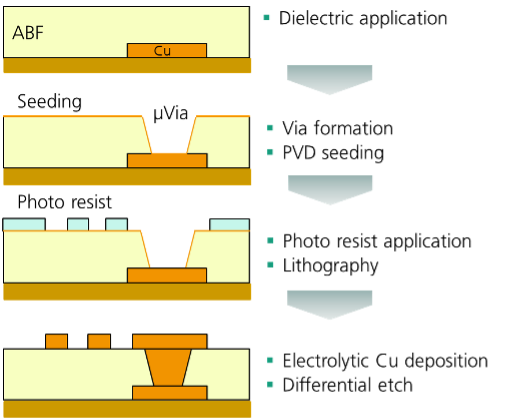
After applying the thin dielectric material, the vertical connections, are formed. A Ti/Cu layer is then sputtered onto the front of the substrate. In a double-sided process, this is also repeated on the reverse side. A thin dry film photoresist is then applied. Direct imaging is used for exposure. The RDL structure is defined in this step. This is followed by electrolytic copper plating, in which the conductive paths are built up. Finally, the photoresist is removed and the copper and titanium layers are etched differentially.
Vertical Interconnects
Various methods for producing the vertical connections, the microvias, are being considered (Figure 2).
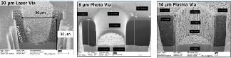
- Laser via is an established method derived from HDI substrate production. However, this technology has limitations in terms of the minimum diameters that can be achieved. In addition, the throughput is limited due to the serial processing of each individual via.
- Photo via in photoimageable dielectrics (PID) are an interesting new approach in substrate technology. They can enable higher resolution as well as fast and parallel processing.
- Plasma, RIE etched, via, combine a photo and a plasma etching process. Here, a lithographically produced mask is used for the plasma etching of the vias. The advantage of this approach is that it aims to achieve similar via dimensions as the photo-via process. Challenges are the still relatively low etch rate, the effect of polymer repositioning and the need for fluorine gases for the process.
RDL formation
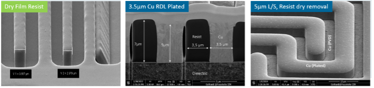
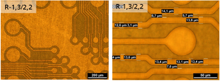
After PVD seeding, a high-resolution photoresist is applied to the substrate. Exposure is carried out using suitable digital direct exposure methods. The target resolution here is 5 µm L/S and below. After the photoresist has been developed, electrolytic copper plating with ultra-fine lines is carried out. To finalize the RDL structure, the photoresist must be removed and the seed layer of Cu and Ti differentially removed (Figure 3). If necessary, the via and RDL formation are carried out in sequence for a further layer.
EU Project CHARM
As part of the CHARM project, IZM, in close cooperation with AT&S, was responsible for the development of a first-level interconnect technology that realizes a high-performance computing module for use as an ADAS system in autonomous mining vehicles.
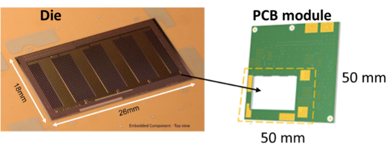
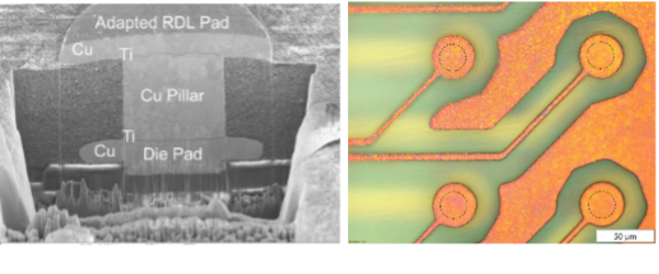
These modules integrate power management, central processing units, memory and thermal management in a very small volume by combining advanced PCB technologies, high-density interconnects and component embedding. For the computing module within the ADAS system, AT&S embedded a large 26x18mm² die using core and ABF materials to form a 150µm thin panel. Vertical interconnects in this approach are formed by Cu pillars on the die, which penetrate through the ABF material and are then exposed in the surface. To provide the first level interconnect for this module, IZM’s challenge was to develop a technology that could accommodate the high I/O count on the die and the given pitch in combination with the required routing density.
For the complete ADAS PCB module, the computing module is stacked on a PCB along with the power supply and memory (Figure 4).
Adaptive Imaging Method
To realize fan-out RDL of fine pitch embedded components, it is essential to use a method that compensates for possible component misalignment, which could be the result of component placement tolerances and displacement during the embedding process. Therefore, it is necessary to adapt the design data used to image the RDL structures. This method requires two main steps:
- Measurement of the given positions of the components on the panel after placement and embedding
- Adaption and recalculation of the design data
- Generation of raster imaging data (RIP)
Based on the above, direct imaging could be performed by digitally imaging the RDL structures using adapted designs.
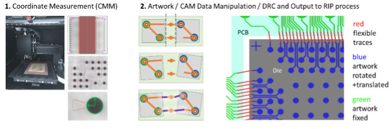
Coordinate measurement and layout adaption
The goal of the coordinate measurement is to obtain reliable x/y/theta measurement data of the components after embedding to ensure accurate and precise results. The measurement is based on a high precision optical coordinate measuring machine (Rudolph/Onto Firefly 1200S). It is crucial to ensure that the substrates are properly illuminated and in optimal surface condition to guarantee the reliability and reproducibility of the measurements. Therefore, it is essential that the marks on the substrate and the components have ideal contrast, which is affected by the opening of these marks and the illumination.
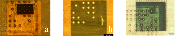
To determine the optimal method for opening the marks, we investigated a number of techniques, including lithography, etching (both wet and dry), and laser ablation. Figure 6 illustrates the results.
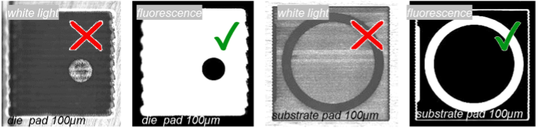
For optimal illumination, we recommend the use of fluorescent lighting. This will allow us to clearly visualize the contour of the metal die pad and registration marks with high contrast (white = organic/ABF/laminate, black = metal/Cu). Please refer to Figure 7.
The measurement data is fed into a CAM-connected script that recalculates the layout on a GBR or ODB basis for each die and all surrounding conductors, traces, and vias for each module. The data set is then imported into a CAM program and checked for design rule compliance (DRC) and error checking of the adaptation routine, Figure 8. Thousands of elements (connections, pads, vias) have to be processed during this step. By optimizing the algorithm, the time required for each module to be calculated has been reduced from several hours to minutes.

Raster image processing (RIP) and lithography
In order to create the necessary exposure data for direct imaging, it is essential to convert the processed, adapted layout data into rasterized machine data. This process results in the creation of a unique RDL data set for each panel processed. The processing time is significantly affected by the resolution and number of elements, as well as the computing power of the RIP engine. The rasterization time for each row of four dies was 20 minutes, resulting in a total rasterization time of 80 minutes for a complete panel. Subsequently, direct imaging was conducted using the registration mark positions from the AOI. Finally, illumination of the panel, which took approximately 15 minutes for one panel, was completed.
Given the significant impact of the seed layer’s roughness on the lithography tool, a series of experiments were conducted to optimize the digital compensation, fluence, and autofocus settings. This was done to achieve a compensated ideal line and space ratio on the modified surface. The optimization loops yielded the results depicted in Figure 9. Reduction values of up to 2.2 µm were employed in both the x and y directions. This outcome can be attributed to the disparate impact of the surface roughness of the copper on the optical system of the exposure unit in the x and y directions. Consequently, it is evident that a more substantial reduction of the structures is essential in the y direction due to this property.
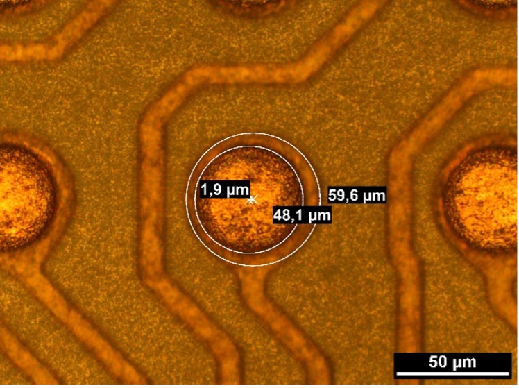
The rasterization of the adapted data of each functional panel with embedded dies was performed in accordance with the specified settings. This resulted in a superior alignment accuracy of the RDL image to the embedded component, with a maximum deviation of 2–6 µm (Figure 10). The necessary 5 µm L/S resolution was achieved using a 7 µm thick dry film photo resist.
RDL formation
The RDL formation was then completed by Cu plating, resist removal and seed etching as described in the first part of this paper. For the project demonstrator, a double-sided SAP process was performed on 610x457mm² panels with 150µm thickness. In total, 9152 I/O pads of the 26x18mm² dies had to be connected to the fan-out RDL structure.
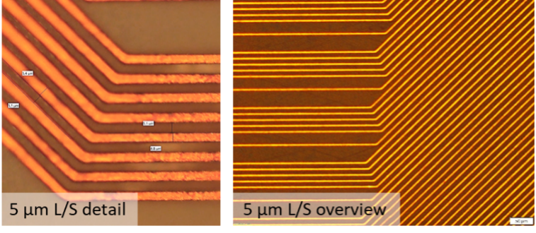
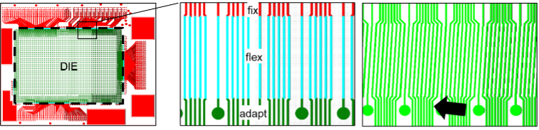
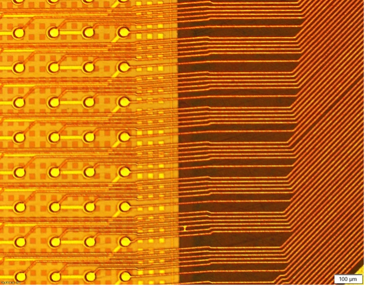
Figure 11 shows a snapshot of the 5µm L/S fan-out RDL required for the CHARM demonstrator. In addition, Figure 11 shows the excellent alignment of the adapted RDL to the die pad and an example of the adapted RDL lines connecting the die pads to the fixed RDL areas.
To complete the final demonstrator, an adaptive fan-out RDL process was successfully implemented.
To successfully fabricate the demonstrator, the development of the core steps for adaptive imaging: measurement of die shift and rotation, processing of adapted layout data, and rasterization of imaging data for exposure was essential.
To obtain the necessary data the die positions on each panel were measured after placement, embedding, pillar reveal, and sputtering. Adaptation of the design data stack resulted in the formation of unique packages and panels corresponding to the real situation of each individual panel.
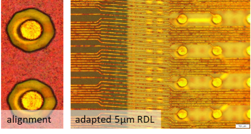
Direct imaging was performed using the adapted true layout data, followed by completion of the fan-out RDL by ultra-fine line Cu plating, resist strip and seed etch. Final results are presented in Figure 13 and Figure 14.
Summary
The development of a process technology for high density organic substrates, based on advanced semi additive processing was successfully demonstrated. Different technology blocks for vertical and horizontal interconnects were established, and the advantages and disadvantages of the different via technologies were determined as a result. In addition, the RDL processing was optimized and alternative process option implemented.
Within the EU project “CHARM”, a successful development of RDL processing for fine L/S structures, which is of paramount importance for fan-out embedded modules with high I/O dies inside, as well in general for HDI substrate manufacturing was achieved. The work done has firstly developed all the core steps for RDL processing, namely the adaptive imaging taking into account the die shifts and twists, rasterization of the imaging data and the final implementation of direct imaging in combination with profound semi-additive processing, reaching even copper structures at 3.5µm L/S. In turn, the developed RDL processes were successfully demonstrated on the computing module manufactured by AT&S, where on one computing panel with four large dies, very fine copper structures at 5µm L/S were achieved as required in the compute module. The R&D work on RDL processing will further build on the CHARM latest results toward even finer L/S structures at high yield for large industrial format panels.