
John Park, product management group director, of Custom IC & PCB Group at Cadence, is a go-to authority on advanced packaging, as I learned as he and I talked about the world of 3D ICs or 3D Heterogeneous Integration (3DHI).
His extensive background in packaging, not chips, was fortified early in his career when he did analog and digital chip design and developed advanced packaging design tools and methodologies. Long-timers will remember Cadnetix, a long-gone EDA company from the 1980s where he worked in the engineering group in Boulder, Colo., where he continues to reside.
Come along as John takes us on an adventurous trip through the world of, as John calls it, 3DHI.
Smith: Why is 3D-IC (aka 3DHI) one of the hottest topics in the semiconductor industry?
Park: The world of the package designer has changed dramatically in the past few years. Packaging has gone from an afterthought to a critical piece of the puzzle for virtually all semiconductor products. All this is due to the interest in multi-chiplet 3D architectures, driven by the perception or truth that we’re at the end of Moore’s Law.
Regardless of what you think, we can all agree that companies following Moore’s Law for their next-generation products is not the best economical path forward nor the best technical path forward. That’s why we’re talking about 3DIC and heterogeneous integration in chiplet-based architectures as the most viable option to scale beyond Moore’s Law and into More-Than-Moore. That is, packaging engineers will disaggregate everything into smaller, modularized building blocks or chiplets.
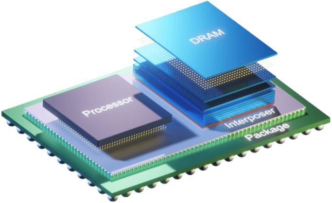
The advantage is we can design an IO or a memory chiplet, for example, and we don’t have to design it at advanced nodes where it costs way too much money to do so. We can build chiplets in different nodes and integrate them together on a single package. That’s why it’s called heterogeneous integration—because a memory chiplet can be designed at 28nm with a CPU designed at 5nm that can be integrated with an IO design at 10nm, all in the same design.
The common term used now is 3DHI, which is a shift from the term, 3D IC. The leading factor driving 3DHI is the high cost of design. A company designing lower volume products cannot compete today designing 5nm and 3nm chips because it costs millions of dollars and requires hundreds of highly trained engineers who are, quite frankly hard to find.
Five years ago, cost forced companies to start to move to 3DHI based purely on the fact that they cannot recoup the non-recurring engineering (NRE) costs associated with designing at the most advanced nodes. Aerospace and defense and other medium-to-low-volume products are leading this push. Another example is hyper scalers, or the high-compute area, running out of space to build their chips as they try to cram more functionality into a single monolithic device. Designers are reaching the max reticle limit, which is the maximum physical size of what can actually be built by the foundry.
10 years ago, a large FPGA company took an FPGA that wasn’t yielding and broke it into four smaller partitions, and put it on a silicon interposer. The reason they did this was that they realized that once big chips moved toward the max reticle limit, they didn’t yield, which means that you can’t ever build the product. This was probably the beginning of 3DHI.
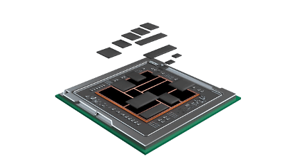
We see other anomaly cases that have to do with form factor. For example, companies build devices that go into something implantable in the body or in eyeglass frames where they don’t have the space or need a different form factor. Therefore, designers start putting smaller chips together and stacking them vertically because they have more space in the vertical direction as opposed to expanding horizontally. This isn’t mainstream at this point, but there are different reasons that companies are moving away from monolithic chips to modularized chiplet-based architectures.
Smith: Wouldn’t the design and verification be more challenging than a monolithic chip?
Park: All this is challenging and I don’t want to make any of it sound simple. You bring up probably the most challenging part of moving into the world of 3DHI, and that is the complexity of the design flow. Essentially, system designers, the people who have historically designed PCBs and multi-die packages, have a set of tools and methodologies. Their needs are converging with IC designers moving to 3DHI.
All of a sudden, a designer who has designed monolithic chips doing static timing analysis (STA) and signoff design rule checking (DRC) is designing systems with multiple chiplets. It’s not STA anymore. He or she has to validate the compliance of the chiplet-to-chiplet interconnect, a signal integrity problem that’s been done for decades on the PCB side, and multi-die packaging.
Now, a different level of expertise and a bunch of extra tools are required. Designers taping out chips are experts in what they do, and they have huge design teams who can write scripts around integration. At one point, they may have had six tools in their flow, and now they have 12 because of this convergence of system design tools with IC design tools.
Thermal analysis is a good example. Moving off a monolithic chip into 3D stacking takes a thermal expert to determine how heat will escape from the chiplet. The complexity of the design flows for 3DHI is double what they were for monolithic chips.
Smith: Packaging was always the last thing chip designers cared about. Is the entire design and packaging world coming together?
Park: That’s it exactly. Going back even a little further than that, package design was a necessary evil. A designer put a chip or die into a package to protect it and to spread the IO out so the board designer could use it.
It’s gone from “do no harm”, and “don’t spend a nickel and do no harm” to the die to the point that packaging is now the differentiating technology for next-generation products. Packaging’s gone from not even an afterthought to being the center of the universe.
As part of the package design community, I spoke at 20 conferences this year. In the past, and before all this took off, I spoke at two conferences a year. The appetite for content on 3DHI is very indicative of this increasing trend.
Smith: You advocate for Assembly Design Kits (ADKs) for 3DHI. How would you describe ADKs?
Park: A Process Design Kit (PDK) is something provided by the foundry to the die designer and a necessary source of data that provides an ASIC designer with the confidence that what they build in their EDA environment can actually be built.
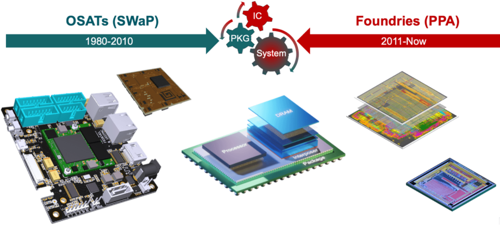
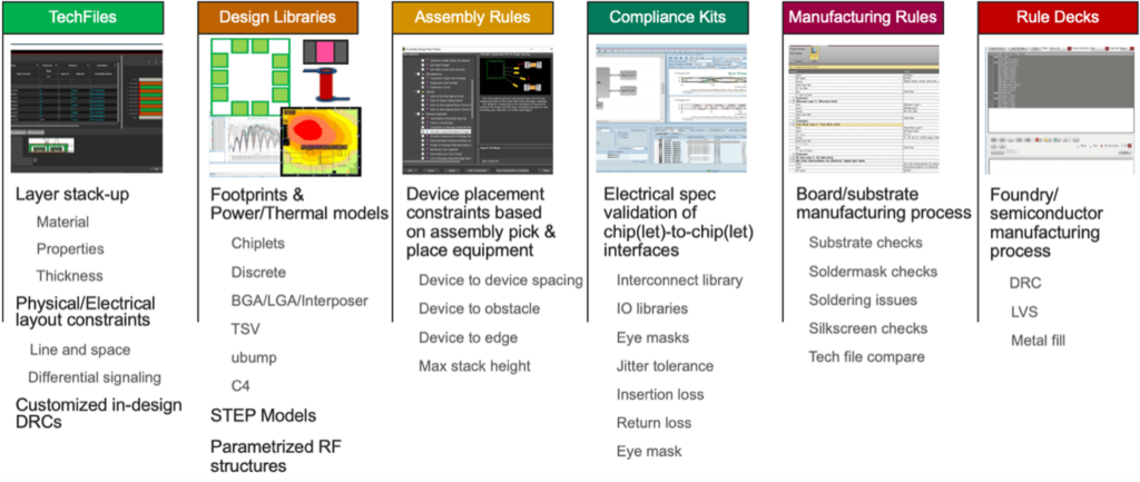
Now that packaging is becoming more complex, ADKs can become the equivalent of PDKs for packaging. When starting a new package, it’s lucky to get an email from whichever company is going to build it, do the assembly, and test. It’s informal—no libraries, no tech files, no design for manufacturing (DFM)—nothing.
For outsourced semiconductor assembly and test providers (OSATs) who build devices, they have to hire huge design teams because it’s an iterative process and an inefficient use model that can’t continue. The packaging world needs to do things like the IC industry with a set of data from the OSAT or foundry that includes technical information.
Some rules will describe the pin pitch of the solder balls of the ball grid array (BGA), and surface-mount components. Other ADK components might include libraries of chiplets, SMDs, and 3D STEP models. The “A” in ADK is the key. We’re not designing a single monolithic chip in this case. We are designing a package that might have 15 chiplets, for instance. And validating the placement of these devices is key to building a product that can be automatically assembled by the OSAT or foundry, driving down the cost of the product substantially.
Smith: What are some of the 3DHI trends you’re seeing as we move into 2023?
Park: I would say there are a couple of trends. If I look at 2023, we’re going to start to see big foundries and OSATs providing robust ADKs. Beyond that, companies will start to invest more time and effort in developing their 3DHI methodology as a robust and streamlined design methodology will be key for designing state-of-the-art, differentiated 3DHI products. These flows will need to seamlessly integrate both IC design tools and system design tools.
Smith: What about industry organizations?
Park: The Open Domain-Specific Architecture (ODSA) within the Open Compute Project is working on chiplet-to-chiplet communication standards, and out of that group came the Bunch of Wires (BOW) specification, a chiplet-to-chiplet communication interface.
In addition, the emerging Universal Chiplet Interconnect Express (UCIe) is an open specification for a die-to-die interconnect that is backed by some of the biggest companies in the semiconductor industry. This standard could potentially enable a chiplet marketplace where chiplets are widely available to the industry.
Additionally, a large foundry recently announced a new technology that consists of a standard language for exchanging full 3D-HI designs across multiple products. I expect to see this standard really take off in the coming months.
We’ve made a lot of progress over the past few years, and we’ll see this trend continue in 2023 and beyond. It doesn’t mean we’re 100% there, but there’s a lot going on when it comes to standards for 3DHI architectures. I’m looking forward to the continued evolution.