
21 ECP tools ordered by top-tier Chinese foundry and multiple advanced package houses
FREMONT, Calif., Feb. 17, 2022 (GLOBE NEWSWIRE) — ACM Research, Inc. (ACM) (NASDAQ: ACMR), a leading supplier of wafer processing solutions for semiconductor and advanced wafer-level packaging (WLP) applications, today announced purchase orders for 13 Ultra ECP map and 8 Ultra ECP ap copper plating systems, of which 10 tools are repeat orders from a top-tier Chinese foundry. The orders represent the first volume purchase order of ACM’s Ultra ECP map systems. The customer has qualified the Ultra ECP map tool in 65 nm to 28 nm processes, where its performance met or exceeded requirements, and has ordered a significant number of tools for its production lines.
“We are thrilled to announce the first volume production orders for our ECP map tools, and additional orders for our ECP ap tools,” said Dr. David Wang, ACM’s President and CEO. “We believe these orders, along with our recently announced wet bench volume orders, demonstrate ACM’s market leadership across a wide range of process technologies and highlight our ability to support our customers’ needs. We are confident that our strategy to broaden our tool portfolio with high-performance tools can help us to capture additional market share in the global semiconductor capital equipment market.”
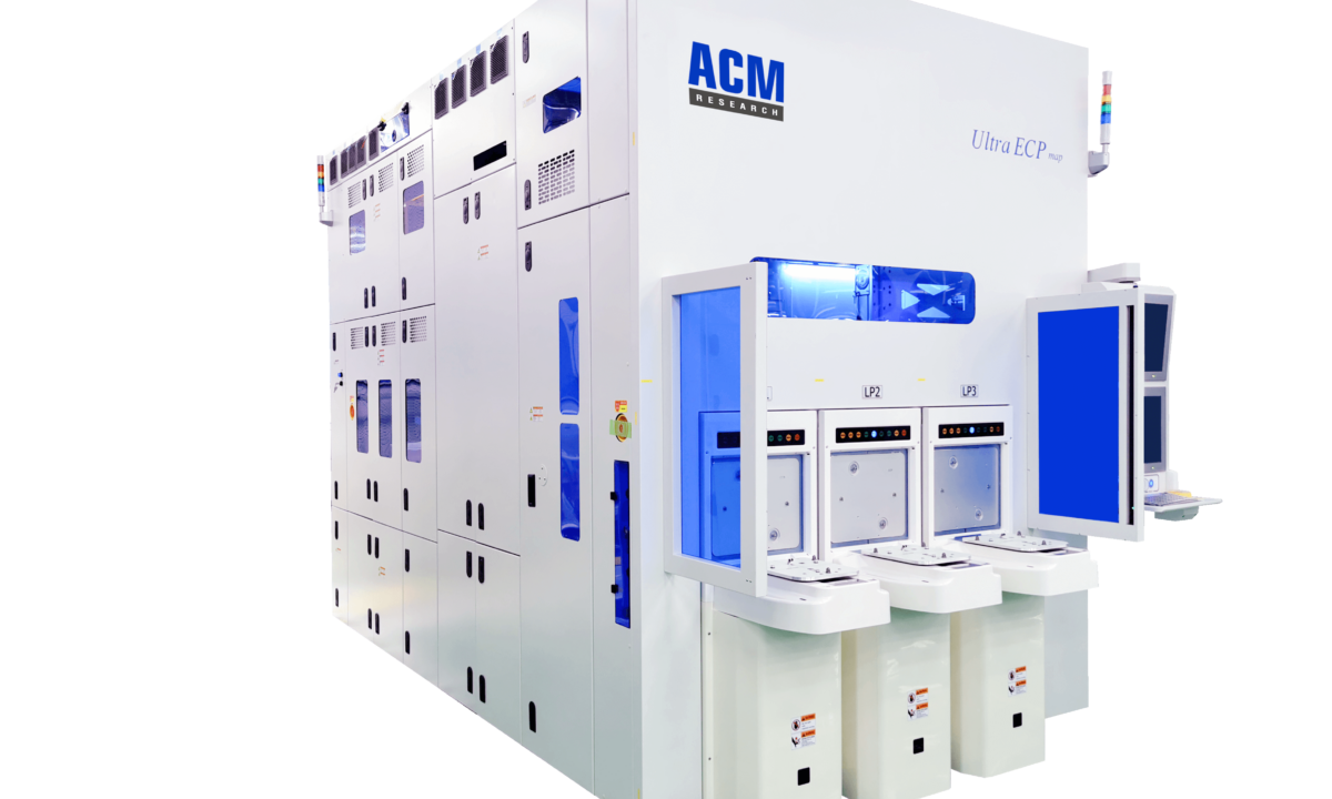
ACM’s Ultra ECP map tool builds on ACM’s electro-chemical-plating (ECP) technology and is designed for dual-damascene applications to improve yield and reliability. ECP plating systems are configured with ACM’s proprietary multi-anode partial plating function, which gives customers a high level of control over depositing the copper metal layer onto dual-damascene structures. Some of the tool’s key process features include its gap filling capability and uniform metal thickness within wafer and wafer to wafer. The tool is compatible with ultra-thin seed layers less than 5 nm, which satisfies the need for dual damascene plating at the most advanced nodes and delivers high throughput and uptime with a lower cost of consumables and lower cost of ownership.
ACM’s Ultra ECP ap plating tool performs many critical WLP plating steps, including bumping and high density fan-out (HDFO) processes, using ACM’s proprietary high-speed plating and second anode technology. The systems provide fast, uniform plating using a specially designed process chamber that provides a strong and steady flow. The single-wafer, flat-type plating design eliminates cross-contamination between chemical baths in vertical-type plating design. The tool delivers excellent performance in Cu, Ni, Sn, Ag and Au plating processes.

About ACM Research, Inc.
ACM develops, manufactures and sells semiconductor process equipment for single-wafer or batch wet cleaning, electroplating, stress-free polishing and thermal processes, which are critical to advanced semiconductor device manufacturing and wafer-level packaging. The company is committed to delivering customized, high-performance, cost-effective process solutions that semiconductor manufacturers can use in numerous manufacturing steps to improve productivity and product yield. For more information, visit www.acmrcsh.com.


