JISSO JOINT consortium
In late 2019 Showa Denko bought Hitachi Chemical (HC) for about $8.9B. HC had an operating income of about $440 million on sales of $6.3B with about 40% of its sales from materials, including chemical mechanical planarization slurries, epoxy compounds, and anode materials for lithium-ion batteries. The company also makes auto components, batteries, and printed circuit boards. Showa Denko had an operating income of $1.7B on sales of $9.1B in 2018. The company makes petrochemicals, building materials, and industrial gases in addition to electronic
In 2018, SDM established the “JOINT (Jisso Open Innovation Network of Tops)” consortium at the Packaging Solution Center to provide solutions for semiconductor packaging materials, equipment, and processes by promoting collaboration with other companies.
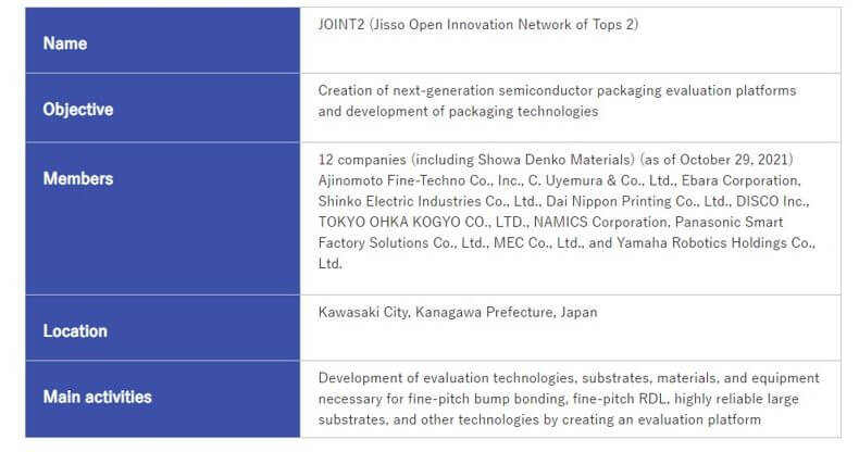
This past October, Showa Denko Materials (SDM) announced the establishment of the JOINT2 (Jisso Open Innovation Network of Tops 2) consortium comprised of 12 companies developing semiconductor packaging materials, substrates, and equipment based in Kanagawa Prefecture.
JOINT2 will form multiple working groups among its members, bringing their expertise through open innovation to develop next-generation semiconductor packaging solutions (Figure 1).
DNP Glass Interposer
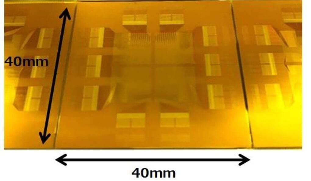
In December JOINT2 consortium member DNP announced that it had developed a glass interposer for next-generation chiplet packaging (Figure 2).
Working with the other JOINT2 member companies, DNP will reportedly further develop the interposer with the goal of mass production in 2024. The DNP glass interposer, shown above, measures 40 x 40mm.
Samsung/Amkor team for Next-Gen H-Cube
Samsung Electronics has recently announced that it has teamed with Samsung Electromechanics (SEMCO) and Amkor on its next generation of H-Cube 2.5D packaging.
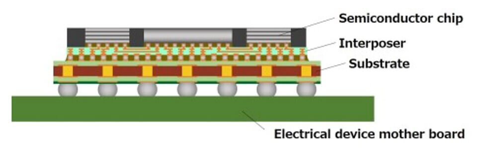
H-cube is being developed for HPC, AI, data center, and networking chiplet designs. H-Cube technology enables logic chips or high-bandwidth memory (HBM) to be placed on top of a silicon interposer in a small form factor. Samsung’s H-Cube technology features a hybrid substrate combined with a fine-pitch substrate which is capable of fine bump connection, and a High-Density Interconnection (HDI) substrate, to implement large sizes into 2.5D packaging.
When integrating six or more HBMs, the difficulty and cost of manufacturing the large-area substrate increase rapidly, resulting in decreased efficiency. Samsung solved this problem by applying a hybrid substrate structure in which HDI substrates that are easy to implement in large-area are overlapped under a high-end fine-pitch substrate.
By decreasing the pitch of solder ball, which electrically connects the chip and the substrate, by 35 percent compared to the conventional ball pitch, the size of fine-pitch substrate can be minimized, while adding an HDI substrate (module PCB) under the fine-pitch substrate to secure connectivity with the system board.
In addition, to enhance the reliability of the H-Cube solution, Samsung applied its proprietary signal/power integrity analysis technology that can stably supply power while minimizing signal loss or distortion when stacking multiple logic chips and HBMs.
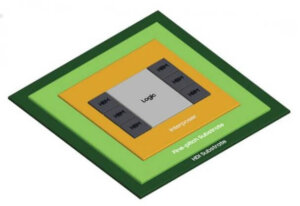
H-Cube solution is suited to high-performance semiconductors that need to integrate a large number of silicon dies (Figure 3).
JUMP 2.0
DARPA MTO has announced DARPA participation in a new long-term university research collaboration with the SRC (Semiconductor Research Corp) and a consortium of companies from industry, as well as the DIB (defense industrial base), called the Joint University Microelectronics Program 2.0 or JUMP 2.0.
The program will support high-risk, high-payoff research that addresses existing and emerging challenges in information and communication technologies (ICT). JUMP 2.0 builds on the agency’s history of supporting long-term, pathfinding university research through public-private partnerships that drive disruption in microelectronics.
JUMP 2.0 will support research that addresses new and emerging challenges facing microelectronics and other information and communications technologies as outlined in the Decadal Plan for Semiconductors.
SRC is seeking proposals from research institutes and universities for seven research center themes:
- Cognition: Next-generation AI systems and architectures
- Communications and Connectivity: Efficient communication technologies for ICT systems
- Intelligent Sensing to Action: Sensing capabilities and embedded intelligence to enable fast and efficient generation of actions
- Systems and Architectures for Distributed Compute: Distributed computing systems and architectures in an energy-efficient compute and accelerator fabric
- Intelligent Memory and Storage: Emerging memory devices and storage arrays for intelligent memory systems
- Advanced Monolithic and Heterogenous Integration: Novel electric and photonic interconnect fabrics and advanced packaging
- High-Performance Energy Efficient Devices: Novel materials, devices, and interconnect technologies to enable next-generation digital and analog applications
A proposers’ day workshop took place on Jan. 25th. The selection of winning proposals is expected to occur on Aug. 23rd. JUMP 2.0 centers are expected to start up by January 2023.
For all the latest in advanced packaging stay linked to IFTLE…………………………………