

Xperi Licenses Hybrid Bonding Technology to YMTC (Yangtze Memory Technologies Co)
In October, Xperi announced it had licensed its hybrid bonding portfolio to YMTC, part of the Tsinghua Unigroup in China.
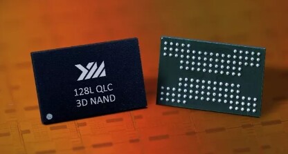
TechInsights had previously confirmed that YMTC is using hybrid bonding in its 128-layer 3D NAND products (Figure 1).
YMTC, headquartered in now-infamous Wuhan, is China’s first producer of flash NAND.
TechInsights reports from their teardown analysis that YMTC uses technologies such as through silicon vias (TSVs) and hybrid Cu-to-Cu bonding technology. The NAND array is upside-down on periphery circuits. The process integration consists as (1) Metal 1 through Metal 4 for periphery circuits on a wafer, (2) NAND array with a source plate (SP) and Metal 1’ through Metal 3’ on a separate wafer, (3) Wafer-to-Wafer bonding to connect M4 and Metal 3’, (4) Through SP Via and Metal 5. Here, Metal 1’ is for BL. NAND array die substrate is very thin comparing with peripheral circuitry die due to a thinning process after hybrid-bonding. So, it is basically leveraging its “Xstacking 2.0 hybrid bonding technology” to essentially bond together the TLC NAND array and the CMOS peripheral circuitry.
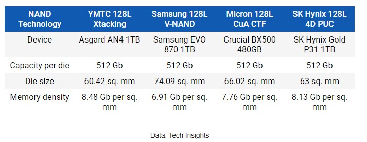
Figure 2 shows comparisons to 128-layer Micron, Samsung and Hynix products.
YMTC, reports an extensive list of clients, mainly Chinese phone makers and SSD manufacturers. With this new 128-layer stacked NAND, the company says it intends to penetrate the data center market in the near future.
YMTC has also been working on a successor to Xstacking 2.0, which will allow the company to make high-capacity QLC 3D NAND memory with a capacity of 1.33 Tb per die. However, development on 128-layer QLC NAND has reportedly been slow, and the company says it has yet to achieve yields needed for mass manufacturing of the new memory chips.

The Big Three; Samsung , Micron and Hynix all moved on (about a year ago) to so called QLC 3D NAND. For instance, in July 2021 Micron announced it began volume shipments of the world’s first 176-layer NAND Universal Flash Storage (UFS) 3.1 mobile solution. This technology allows 5G phones up to 75% faster sequential write and random read performance than prior generations, enabling downloads of two-hour 4K movies in as little as 9.6 seconds.
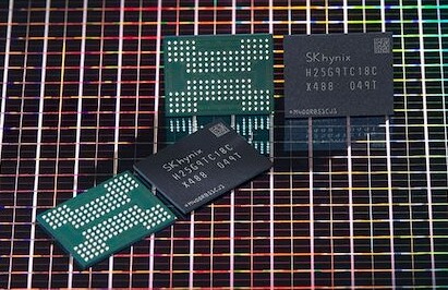
Hynix had similar announcements in Dec 2020. The maximum IO speed between NAND dies and the SSD controller has been increased from 1.2GT/s for their 128L NAND to 1.6GT/s for the 176L NAND (Figure 3).
For all the latest in Advanced Packaging stay linked to IFTLE………………………………………


