
Watching the Intel Accelerated event recently brings to mind one of my favorite movies of all time: Rocky. Let me share the fact that Sylvester Stallone (3 years older than I am) and I actually grew up in the same NYC neighborhood, Hell’s Kitchen (he later moved to Philly).
At first, you may say, “That’s crazy Rocky was an underdog story and Intel was never an underdog,” and you’d be correct about that. What I’m focusing on, however, is that last fight of the 1976 movie where Rocky is being pummeled by Apollo Creed (current champion) and suddenly turns the fight around and ends up winning and wrapping himself in the American flag.
In the past few years, we can all agree that Intel has certainly taken a verbal pummeling from all sides of the industry with the consensus opinion being that they just couldn’t keep up anymore with the likes of TSMC and Samsung and were hopelessly falling behind and in danger of becoming an also-ran.
But in 2021, Intel CEO Pat Gelsinger, like Rocky, refused to accept this position and instead came out swinging. IFTLE recently reported on Intel’s discussions to buy GlobalFoundries (GF) and its announced partnership with IBM R&D. (see IFTLE 492: “Will Intel Acquire GlobalFoundries? Intel/IBM R&D Partnership.”)
This news sent shock waves through the industry and, as I said a few blogs ago, would be just what Intel needed to become a heavyweight in the foundry business. In addition, what better time to battle back to the front of the pack than when the US is focused on “on-shoring” chip manufacturing and advanced component packaging?
Intel Accelerated Event
With that said, let’s get to the main topic of this blog, which is the July 26th “Intel Accelerated” event delivered by Gelsinger and his team. They laid out a roadmap to expand Intel’s foundry business to catch rivals TSMC and Samsung by 2025.
Intel described coming innovations in semiconductor front-end processes and back-end packaging, which they had previously only alluded to as IDM 2.0 earlier this year.

Gelsinger announced that Intel is investing to become “a world-class foundry business and a major supplier of US and European based capacity to serve customers globally.” and reported that they have spent 3.5B$ in their New Mexico facility to support advanced packaging.
The naming of nodes is being changed at Intel. As IFTLE has discussed previously [IFTLE 462: “If not nodes then what?”] process nodes were originally named after the gate length in nanometers.
Since 1997 other Intel innovations such as strained silicon became equally important to making the transistors faster and more energy-efficient (Figure 2).
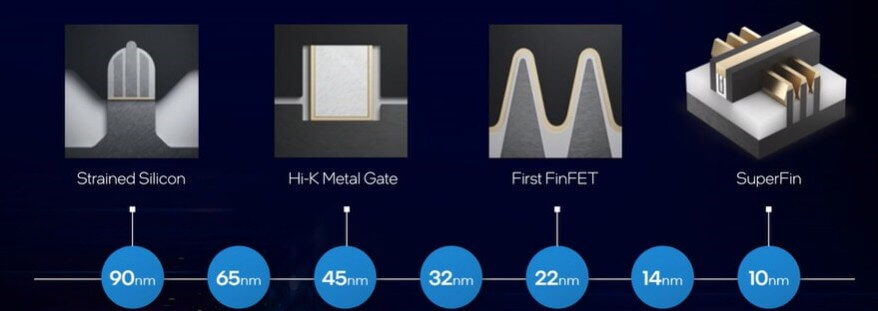
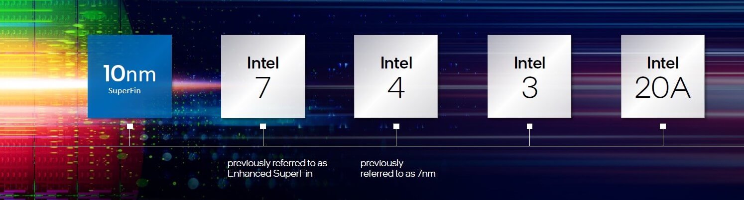
This is when naming stopped being directly linked to the actual length of the transistor gate. This became even worse in 2011 with the introduction of FinFET transistors which were entirely new structures. So numbering systems cannot be compared between companies nowadays. Intel will be changing naming for everything past the 10nm super fin as shown below.
Kelleher reported that we can expect the following process improvements:
- Intel 7 (previously 10nm Enhanced): The 10nm super fin technology is now ramped into volume production in Oregon, Arizona, and Israel. They are currently manufacturing more 10nm wafers than 14nm wafers.
This technology should deliver approximately 10% to 15% performance per watt increase over Intel 10nm Super Fin through FinFET transistor optimizations, including increased strain, low-resistance materials, high-density patterning techniques, better routing, and a higher metal stack. “Alder Lake” will begin shipping in late 2021 followed by “Sapphire Rapids”, both using Intel 7.
- Intel 4 (previously Intel 7nm) – this technology should provide an approximately 20% performance per watt increase over Intel 7, Intel 4 is the first Intel FinFET node to use ASML extreme ultraviolet lithography (EUV). Intel 4 will begin shipping in 2023, in products such as “Meteor Lake” and “Granite Rapids”.
- Intel 3 – Early modeling indicates that Intel 3 will reportedly deliver around an 18% performance-per-watt increase over Intel 4. Intel 3 will be ready for manufacturing products in the second half of 2023.
- Intel 20A – This is expected to be introduced in the first half of 2024. This will mark the beginning of the “angstrom era” in semiconductors where manufacturing processes will move beyond 1nm. It will include two breakthrough technologies, PowerVia and RibbonFET.
PowerVia will involve so-called “backside power delivery, instead of routing power through the front of the wafer. By eliminating power delivery on the top of the transistors more resources are available to optimize signal routing and lower delays.
RibbonFET will be a gate-all-around (GAA) transistor design. It’s the first new transistor architecture since Intel pioneered FinFET in 2011. It reportedly will improve transistor switching to deliver faster, more efficient processors. This design essentially utilizes multiple gates on the transistor, allowing it to switch faster compared to a single gate.
- Intel 18A – After Intel 20A, the company will move to Intel 18A. Intel 18A is currently in development for post-2025.
Packaging: The Crucial Component
Kelleher also reports that packaging is a crucial component for their IDM 2.0 overall strategy, “…enabling us to …incorporate disparate nodes and processes.”
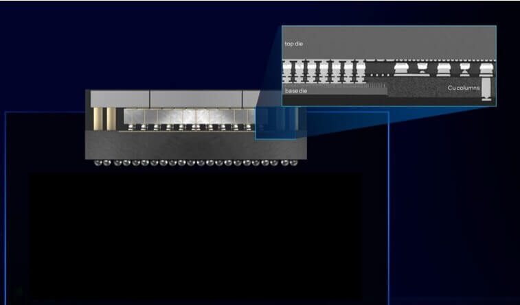
Embedded multi-die interconnect bridge (EMIB) is Intel’s 2.5D solution that has been shipping since 2017. “Sapphire Rapids” will be the first product to ship in volume with EMIB. The next-generation EMIB will scale to 45µm pitch and will then scale to 40 µm in the next generation. 45nm EMIB will be used on a 92 x 92 mm package, the world’s biggest BGA package.

Meteor Lake will use Foveros technology and be done at 36 µm bump pitch.
The Pointe Vecchio CPU will be the first product powered by EMIB and second-generation Foveros.
Kelleher noted that “Many of these innovations and technologies will be available for our foundry customers products.” (exactly which ones was not clarified)
Coming soon are Foveros Omni and Foveros direct (hybrid bonding interconnect)
Foveros Omni should be available for volume manufacturing in 2023. Foveros Omni allows the connection on multiple disaggregated top tiles with multiple base tiles which can be of mixed fab nodes. It uses through-silicon via (TSV) and copper column technology. It uses 35 to 25 µm bump pitch which gives a bump density of 1600 per mm sq.
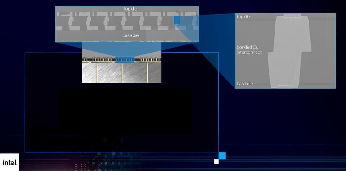
Foveros Direct or hybrid bonding will also be ready for volume manufacturing in 2023. It gives the user sub 10µm bump pitch, solderless direct copper-to-copper bonding, resulting in lower resistance interconnect and a bump density of 10K /mm sq.
Intel also noted that photonics will be incorporated into future generations of its technology and that the company is working with Leti, IMEC, and IBM to further their packaging advances.
Lastly, Gelsinger was quick to point out that they were the only leading-edge player doing both R&D and manufacturing in the US.
Intel reports that its first major foundry customers for IFS (Intel Foundry Services) will be Qualcomm and Amazon.
Qualcomm, which dominates chips for mobile phones, will use the Intel 20A process. It’s not clear how many of Qualcomm’s processors Intel will manufacture. Qualcomm is known to use multiple foundry partners, sometimes for the same chip. For instance, Qualcomm has had its Snapdragon processors made by both Samsung and TSMC. It’s a similar story for Apple. Intel did not give details on how much revenue or manufacturing volume these foundry customer wins would bring.
Does this mean that Intel’s foundries will be making chips for its rivals based on a design from ARM, rather than the x86 architecture that’s at the heart of its processors? That is yet to be determined.
Amazon, which is increasingly making its own data center chips for its Amazon Web Services, is not yet using Intel’s chipmaking technology but will use Intel’s packaging technology.
For all the latest on Advanced Packaging stay linked to IFTLE………………….


