


A Conversation with the Xperi Hybrid Bonding Team
In the world of heterogeneous integration, hybrid bonding — and in particular, Direct Bond Interconnect (DBI®) is quickly becoming the preferred permanent bonding path for forming high-density interconnects in a multitude of applications, from image sensors and MEMS devices, and most recently memory — with RF devices and logic poised for take-off. Since it was first conceived in the mid-80s by Paul Enquist, Q.Y. Tong, and Gill Fountain in the labs at Research Triangle Institute (RTI), DBI has proven to be a game-changer for its elegance and simplicity. It creates a dielectric-to-dielectric bond, and the interconnection is formed by metal-to-metal contact through a low-temperature process.
But DBI is so much more than its technology. The people behind this revolutionary and disruptive process are the real story — from those who first developed it, to those who joined the technology team along the way, and the business and marketing minds who brought it to commercialization. While the technology ownership has changed hands — its original company, Ziptronix, was acquired by Xperi in 2015, and is now part of Xperi’s Invensas semiconductor technology portfolio — the people who first developed and patented the technology are still very much involved. In this exclusive interview, we asked the core DBI team to tell their stories about being part of the DBI journey, the roles they play, the challenges they’ve overcome, and what the future holds.
The Early Days – Paul Enquist and Gill Fountain
Before Ziptronix existed, Paul Enquist and Gill Fountain were already at work developing this hybrid bonding solution at RTI. It began with the ZiBond® direct bonding process and then led to the discovery of forming the interconnect, which became DBI.
As Gill tells it, the RTI team was working on a multichip module (MCM) for a customer that involved integrating memory, a processor, and FPGA on top of DRAM. The complexity of the project had them “tearing their hair out” for over a year. Through the ZiBond process of bonding chips on the face of the DRAM and then using a redistribution layer (RDL) to form the interconnect, Gill and Tong discovered a better approach to RDL. By using plating technology, specifically — chemical mechanical polishing (CMP), they could achieve a flatness that allowed the Ni and oxide to not only bond but form an interconnect. “Everyone thought it was a stunt. Nobody believed the process was reproducible. But it was!” he said. “Later we discovered we could do it with copper.” And so, by happy coincidence, DBI was born.
“Bonding was what we first built the company on,” says Gill, “The holy grail was to have the connection automatically come with the bonding by taking a dielectric and metal surface, polish it flat and make a connection. It was amazing! That was really something for a group of guys from a research background. It was quite a development.”

Paul says it was a matter of being at the right place at the right time, and it was enough to spark the interest of investors. So, after years of building the technology behind both ZiBond and DBI at RTI, it was time to spin out a start-up.
“We got the first round of venture capital funding, took a handful of engineers, and turned them into entrepreneurs,” said Paul. While it took 10-15 years to come to fruition, which was longer than anyone wanted, Paul says it aligns with how long things take in the semiconductor industry. “Founders like Gill have put decades into this. It’s been quite a ride.”
Gill says the first big break for DBI came when Raytheon showed interest. “They saw that DBI would give them not just bonding, but connectivity at the pitch they needed, and they were sold,” he said, “It was a huge break that led to the first technology transfer. We demonstrated we had something real and not just a science fair project. It was a real technology that could have a powerful impact on the industry.”
“It’s one thing when you use your technology, but when other people use it, that’s a great proof point,” said Paul. “That was the first stage of adoption.”
Figuring out how to perform DBI using Cu, so that it could be aligned with standard semiconductor processes was another important milestone, noted Paul. Then the CMOS image sensor market took off, driven by smartphones, and with it a need to scale pixels using bonding technologies. DBI made it possible to make connections between the two wafers. Sony licensed the technology, which was another big break for DBI.
The Acquisition – Craig Mitchell

Craig Mitchell, President of Invensas, a wholly-owned subsidiary of Xperi, says he started watching DBI back in 2003.
“I was keeping an eye on the technology to see if it could scale and be applied to a high-volume market,” he explained. “The Ziptronix team proved that out by working with some pretty big semiconductor manufacturing companies. We could see that this was where the industry was headed and that there would be a need for this type of bonding and interconnect technology that would allow the industry to continue to scale.”
Bringing Ziptronix and Invensas together at the right time meant they could continue building on the foundation that Ziptronix had established. “It’s been continuously exciting,” he said.
“We were a start-up for 15 years, and I didn’t think we’d get out of it,” said Gill. “When Invensas came along, it was a game-changer for all of us. We thought it would never happen. It seems like you just have to hang in there until the time is right.” Becoming part of Invensas opened up the opportunity to expand on many more levels, such as incorporating TSVs into the technology.
The Transfer to Invensas – Guilian Gao and Cyprian Uzoh
Guilian Gao, distinguished engineer, and Cyprian Uzoh, principal engineer, were also involved early in the acquisition process, performing due diligence to evaluate the fundamentals of ZiBond and DBI.
Before joining the DBI team, Guilian worked on the 3D team at Invensas, working on through-silicon via (TSV) integration with solder cap and microbumps, examining the technology fundamentals. Because of this work, she knew it would be hard to scale processes below 40µm. DBI provided a scalable interconnect alternative, and she was very excited about its possibilities.

Cyprian, a research scientist at IBM, was invited by Bel Haba to join Xperi to work on TSVs in 2010. Cyprian drew on his expertise in Cu interconnect technology to review the full patent portfolio, mapping and studying the core patent claims for evidence of use. Cyprian’s inventions, such as bottom-up Cu fill for TSVs, are the core foundation of modern chip interconnection technology. If anyone could tell if this process was going places, it was him.
Guilian was the first person to touch DBI on its journey from Ziptronix in Raleigh, North Carolina to Invensas, in San Jose. She worked with Gill to put together the technology transfer package for both ZiBond and DBI. The situation was a little unusual, as Gill couldn’t travel because of an ankle injury.
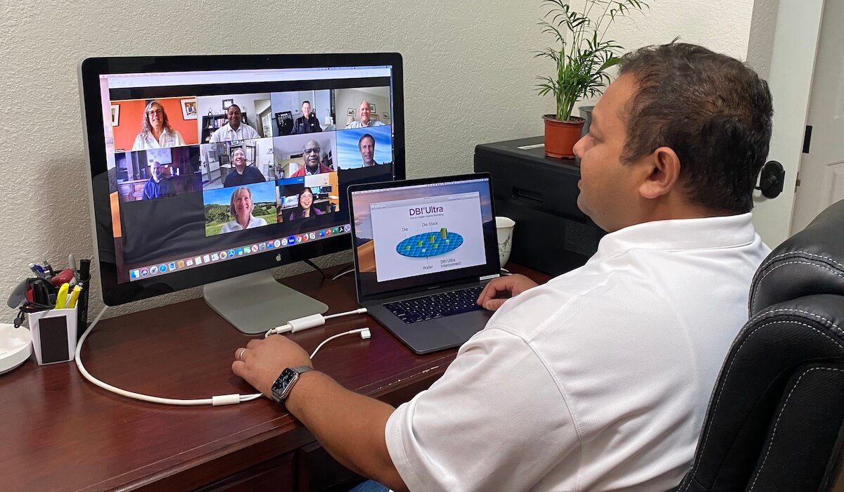
“I was in my home talking to Guilian on the phone and using WebEx, so it was interesting,” he recalls.
“We had lots of daily conference calls because my starting point was low,” said Guilian. “I came from a board assembly background, so it was a steep learning curve for me, but Gill was a very patient and excellent teacher.”
The Next Era of DBI Development – Laura Mirkarimi and Tom Workman

A veteran of Invensas who had left in 2015 for a position at Zeiss Group, Laura Mirkarimi rejoined Invensas as VP of 3D Portfolio and Technology in February of 2016 specifically to lead the R&D development for DBI. “That was my first introduction to DBI and I saw the incredible potential of this clever platform technology,” she said. “It’s not a single point solution, it’s a platform toolkit from which to design features into products. Once you have it in your toolkit, it becomes pervasive.”
Her team works together to address fundamental challenges in DBI, and how to proliferate the technology across multiple applications. This includes internal development and partnerships to ensure the silicon supply chain is ready for the technology.
Together, Gill, Guilian, Cyprian, Tom, and Laura brought up the new Class 1000 assembly lab cleanroom, the level of clean needed for DBI processes. They added back-end-of-line equipment including CMP capabilities and various metrology tools. Every piece of equipment was new and some of it was custom built by “Gill Co.” (the code word for home-built by Gill Fountain, because the necessary tools had yet to be built by suppliers.)
“We brought it up and qualified it. That is how I learned to walk with DBI,” said Guillian. “ I have been in the lab for the past 5 years, doing something new each day. It is never boring. I am a bit like the glue in the 3D group. I know a little bit of everything to be dangerous in the lab. I am a co-inventor on many DBI related patents. I am also a messenger of the technology through publications.”
Through the evaluation process, Cyprian learned what improvements are needed for a manufacturing processes and lower costs. He continues conducting experiments and develop new methods, chemical formularies, new equipment designs, and more. For example, he developed a custom tool to meet the stringent cleaning requirements for die-to-wafer DBI® Ultra processes.
“I was excited about the patents. Cleaning tools needed to be redesigned, so we brought it in-house to make the technology work and reduce the cost,” said Cyprian. His work and pilot operations have led to extensive patent filings.
Laura explained that it was important to understand customer pain points that could be solved by integrating DBI into the process flow. Using solder interconnect and everything to do with it was an ongoing issue that could be solved with DBI.
“We’ve had excellent input from top-tier manufacturers that reinforce where the technology can go. It took a significant engineering effort to get to an HVM-worthy process with a keen understanding on the fundamental physics,” she said. “We started early on with die-to-wafer, but the tools weren’t ready in the semiconductor space. It takes time to get the infrastructure in place and then take off.”

Tom Workman a principal engineer, who joined the development team in 2017, was also drawn to the opportunity to work on DBI. “At Intel, I worked on the C4 bumping process. DBI interested me enough to get me to join Xperi,” he said. “It seemed to be something that takes C4 to the ultimate conclusion — bonding two chips together without intermediary bumping or metallization. It’s exciting to take a genius idea, dig in, and optimize it for HVM.”
Tom works closely with the tool vendors. “Three years ago, it was a tough sell to bonding tool companies to meet the specifications for DBI. But now, it’s the exact opposite,” he said. “These companies are coming to us with test specifications from device companies asking for cleanliness requirements. We’ve become a resource for equipment manufacturers. We have some great partnerships with equipment suppliers where there is motivation on both sides.”
Building the Business – Rick McClellan
On the business side, Rick McClellan, VP of Business Development, says it’s the people at both Ziptronix and Xperi who made it the success it is today. For him, one of the most instrumental people for helping him early on was Kathy Cook, who was his business development colleague first at Ziptronix, and then again at Xperi. Kathy also joined Invensas as part of the Ziptronix acquisition. She has now moved on to another Xperi spin-in — Perceive, where she is VP of Business Development.
“When I first joined Ziptronix in 2013, I was effectively joined at the hip with Paul and Kathy. And I can’t tell you how much they helped me learn and understand the basics, so I could go out and bring the messaging in front of these companies,” says Rick.
After the acquisition, he left to join SK hynix for a spell and then was hired by Craig to work at Xperi in 2017. He was excited about joining an even bigger team of talented people.
What Rick enjoys most is working with Paul, Tom, and Laura on customer engagement. When Tom presented recent findings at IMAPS DPC in March 2020, Rick watched from the background (Figure 5). “He was bombarded by questions. It was exciting to see everyone’s enthusiasm for this technology,” he said. “We’ve got an entire generation of engineers that are thinking and designing in 3D and that’s what has them excited.”
Another story he likes to tell is when he joined Laura and Tom on a visit from a tier-one memory company to the Xperi R&D facility in San Jose. These potential customers were still doubtful about a room temperature bond. “Laura and Tom arranged an entire demo in the cleanroom. Tom went through 60 die-to-wafer placements in real-time and handed them the wafer,” he recalled. “Everyone in the group tried to push the die off of the wafer that Tom had just bonded at room temperature. The die wouldn’t budge. and you should have seen the look on their faces. Needless to say, they are a licensee today.”
Marketing the DBI and DBI Ultra Brand – Abul Nuruzzman

Abul, who is currently VP of Product Marketing, joined the DBI team in 2015 shortly after the acquisition of Ziptronix and has lived it through the merger with DTS and rebrand as Xperi.
“Helping to drive the market success of DBI, as well as oversee the introduction of DBI Ultra was exciting,” said Abul. “We launched die-to-wafer hybrid bonding to the market earlier than anyone, including major semiconductor companies like TSMC, Intel, who followed with similar die-to-wafer market announcements.”
Abul is fascinated by the technology, especially how these micro and nanoscale processes can have such a big impact at the device and system level. He enjoys worked with the technology team to craft the DBI story and creating process flow diagrams and models. “It’s one of the best jobs I’ve ever had,” he says.
Abul says It was a bit of a marketing challenge in the beginning because the Ziptronix brand was so well known. But because the foundational technology brand has remained consistent despite the change in the corporate brand, Abul says the DBI brand story remained stable. “New things happen, things change, but the essence of hybrid bonding and the education process to communicate its core values and performance doesn’t change,” said Abul.
The key, Craig says, is to maintain consistency with the technology brands. “We invest in those brands. Sometimes the corporate brand evolves, but it’s important to maintain the product brands,” he explained.
Abul noted that the product line branding posed its own subset of challenges, as the technology itself evolved. For example, a completely different set of challenges had to be solved to develop the die-to-wafer version of DBI. As such, the team believed it deserved its own brand and came up with the DBI Ultra name.
Big Breaks and Plot Twists
“From the commercial perspective, licensing a company like Sony was a massive milestone,” said Craig. “It set the stage for broader industry to evaluate its potential and apply it to their technology and product roadmaps.” A more recent milestone was licensing the technology to SK hynix for its memory products, as well as seeing it adopted into other high-volume markets beyond image sensors.
“I’m excited to see where things go next,” says Craig. “As DBI finds its way into bigger markets and proliferates into other applications, it opens up the door for the entire ecosystem to embrace the technology. The more people involved, the more we’ll see it applied in other applications. There are exciting milestones still to come.”
“Moore’s Law scaling is so expensive. Only a few foundries are continuing to do it. One way to compensate for that is 3D stacking and scaling,” noted Abul. “That’s why DBI is getting attention in the memory and logic space for high-performance computing.”
“There have been many plot twists over the years,” said Paul. “While the fundamental technology remains stable, lots of things have changed. While investors, customers, business models have changed, the core technology has not. For example, during the Y2K euphoria, investors were throwing money at it and we were lining up customers. Then the bubble burst and we had to adjust the business plan and the story. But the technology got us through.”
“I don’t think the industry fully appreciate the significance of DBI as a room-temperature process,” says Cyprian. He says when he was at IBM working on Watson, they were bonding silicon on insulator (SOI) wafers at 1200°C. “We couldn’t imagine doing that at 200°C. It never occurred to us that we could bond at a low temperature,”
Laura says it’s easy to forget how they felt the first time they looked at DBI. “What amazed me was the simplicity around it and the problems it solved,” she recalls. “It looked so clever. The fact that the bond happens at room temperature and then heat it to enhance the interconnect is beautiful. The physics works.” She added that she could see why companies would want this technology, especially after all the money spent on advanced packaging technologies to come up with an MCM.
“If you can control things to take advantage of bonding at room temperature, you can really start to think about true heterogeneous integration,” she said.
What the Future Holds
“We have so much flexibility with ZiBond, DBI, and DBI Ultra,” said Laura. “We’re going to see so much innovation and new architectures in the memory/logic space. By developing the DBI Ultra, we have the ability to do high volume manufacturing for true 3D integration.”
“Because of this technology, I believe in about 10- or 15-years demand for things like underfill and solder will go down,” says Cyprian. “I believe in the future we’ll be doing Zibond at 100°C, which means we can have polymer materials that are high performance, but because of temperature issues haven’t been able to use them.”
“I see ZiBond and DBI as the tools in the 3D integration toolbox that the industry will rely on for decades to come,” said Craig. “We’re just at the early stages of DBI adoption. We see it in image sensors already — we’ll see it in RF and memory. In logic, the combination of logic and memory, and the disaggregation of devices, DBI can be that core enabling technology that is pervasive throughout the semiconductor space and allows us to scale performance, functionality, cost, power, leveraging the existing infrastructure.
Conclusion
So, there you have it: the DBI story through the eyes of the people who are making it happen. What I loved most about this conversation is that every single person is passionate about the technology, from those who conceived it to those who joined Xperi just for the opportunity to work on DBI. It’s because of all of them that this technology is succeeding. Technologies don’t just happen. It takes people to discover them, realize their potential, and push them to succeed. Paul, Gill, Craig, Guilian, Cyprian, Laura, Tom, Rick, and Abul, – I can’t wait to see where you take this technology next. ~ FvT
This article appeared on the cover of the 2021 Yearbook. Read the issue here.


