It was exactly two years ago that IFTLE first discussed the entity known as BRIDG and how it planned to be a “boutique microelectronics fabrication facility” that would be able to prototype 2.5/3D devices for the U. S. government and the microelectronics community.
Later in the year, BRIDG announced that it had a deal in place with imec to transfer imec’s 2.5/3D technology to the BRIDG facility in Florida and had been joined in their consortia effort by Süss MicroTec and Tokyo Electron.
What is reported to have happened at BRIDG over the past two years is confusing, to say the least, but we will try to straighten that out in this blog. BRIDG was conceived as a non-profit research consortium. For you old-timers, I liken this to the operation started in the 1980s called the Microelectronics Center of North Carolina (MCNC) where I got my microelectronics education. MCNC was a non-profit entity existing in a building owned and facilitated by the state of North Carolina to draw other electronic players into Research Triangle Park.
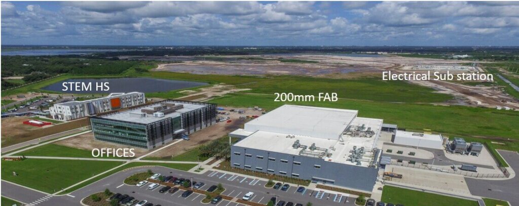
BRIDG is a non-profit, public-private partnership providing customer-funded semiconductor R&D and low-volume manufacturing capabilities for industry, government, and academia. It is enabled by a 109,000 sq ft, 200mm microelectronics fabrication facility in the 500-acre technology district known as NeoCity (see above). Osceola County, Florida, had ownership of the land and fab building and a deal was cut with the University of Central Florida (USF) to run the operation. BRIDG would use the facility to develop processes and products for its customer base.
In Nov of 2019, IFTLE reported that the U.S. Department of Defense’s Industrial Base Analysis and Sustainment (IBAS) office had awarded BRIDG its first major federal defense contract ($20 million) to provide a new technology for “next-generation microelectronic multi-chip systems that will strengthen national security and cyber resiliency for the United States defense industrial base”. But things soon began to turn sour for this fledgling organization.
BRIDG over Troubled Waters?
[For those of you not yet born at the time, this a 1970 Simon and Garfunkel reference and I’m using it because Paul Simon’s father was my English teacher in junior high school, back in my youth, in Hell’s Kitchen in NYC.]
All during 2020 we began hearing about BRIDG “financial issues” and then in the fall, reports were published about a financial crisis. Reports from insiders indicated that UCF couldn’t handle the financial obligations they had incurred and were trying to unburden themselves from their contract. This would leave BRIDG without a facility to work in. By now BRIDG had accumulated more than $60 million in contracts but they were going to be without a fab.
Then, SkyWater Technology and BRIDG established a partnership, to “…accelerate access to domestic development and manufacturing services for microelectronics advanced packaging.” UCF would hand off the remainder of its 40-year lease to SkyWater, which would replace $50 million to $60 million in funding the facility would’ve received from the university for operations and capital expenses over the first five years of the agreement.
In January of 2021, SkyWater announced a public-private partnership with Osceola County, Florida, and BRIDG to accelerate access to domestic development and manufacturing services for microelectronics advanced packaging. Skywater and BRIDG are partners but independent entities. They might do joint work together, but will each have customers for whom they are developing and/or manufacturing advanced packaging solutions.
SkyWater has established a subsidiary, SkyWater Florida, to assume operation of the 200mm semiconductor manufacturing facility that will become the foundation for the company’s leading-edge advanced packaging technology services. SkyWater will utilize the fab to address emerging commercial and government agency needs for U.S.-sourced electronics.
BRIDG currently reports that “Wafer processing will resume as soon as we can safely and efficiently restore operational capability to the facility and the wafer processing tools, hopefully as soon as early Q2 2021. Production is planned to start at the end of 2021”. CEO Brian Sapp reports that the roadmap for BRIDG and the Neocity fab is to have both bumping and redistribution layer (RDL) processes available as soon as possible.
Also of interest to our packaging community is exactly what technology IMEC has been transferring to BRIDG, since we all know IMEC is probably the most prolific 2.5/3D organization in the world. IFTLE went direct to the source and have been told by Eric Beyne of imec and BRIDG’s Brian Sapp that the project has 4 phases (Figure 1), and they are currently at the start of Phase 4. Although there were reports of layoffs during the UCF financial crisis, the technology transfer from imec to BRIDG continued unabated.
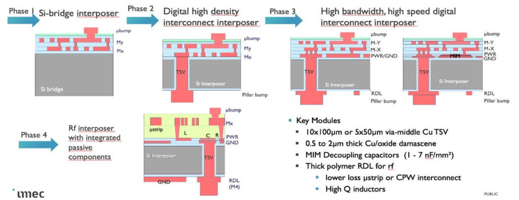
Beyne reports that “We used a modular approach, stepping up from a thick Cu/damascene process (phase 1), adding through-silicon vias (TSVs) (phase 2) to a flow for high-bandwidth digital interposers that also includes metal-insulator-metal decoupling caps between power and ground plane layers (Phase3). The last phase (4) is the addition of a module that allows for very high frequency interconnects. This one uses a low k spin-on dielectric, with a thickness up to 20µm as the main medium for realizing low-loss microstrip and coplanar waveguides with good isolation of the electromagnetic fields from the (regular) Si interposer substrate.” Might that spin-on low-k dielectric be DuPont’s Benzocyclobutene (BCB)? (boy does that sound strange to me)
[Once again, let me interrupt for any youngsters reading this. IFTLE while working for Dow Chemical in the 1990s brought BCB through R&D and into commercialization. Beyne and imec were one of the institutes helping develop BCB processing. During that time DuPont and PI were arch enemies. Though DuPont Electronics was a much larger business, Dow and IFTLE beat them to both RDL and wafer-level packaging. A few years ago, as you may be aware, Dow and DuPont merged into the US’s only remaining major chemical company and then split into 3 parts with DuPont becoming the electronic material supplier.]
To summarize, it now looks like we have a BRIDG to somewhere. We certainly look forward to the day when we have multiple sources of advanced packaging capability onshore.
For all the latest in Advanced Packaging stay linked to IFTLE………………………