


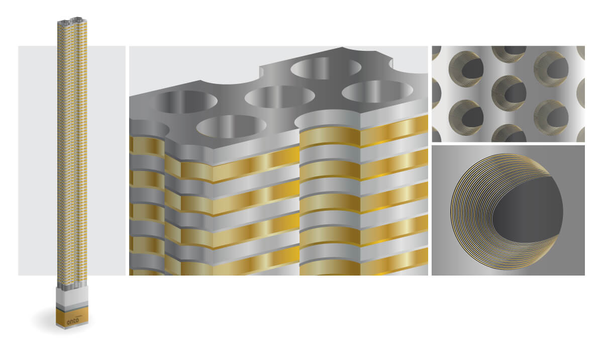
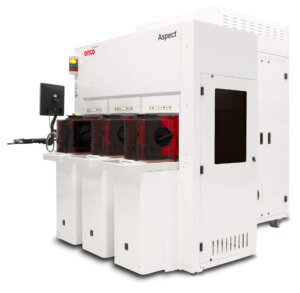
Wilmington, Mass., December 16, 2020 – Onto Innovation Inc. (NYSE: ONTO) today announced the first customer acceptance and purchase of its new product, the Aspect® IRCD System, at one of the top three memory manufacturers of leading-edge 3D-NAND devices. After successful factory demonstrations, additional Aspect systems are shipping this quarter and in the first quarter of 2021 for evaluations at leading 3D-NAND manufacturers. All of these customers are expected to utilize the high-speed capabilities of the Aspect System to accurately measure extremely deep, high aspect ratio channel holes used to connect over 128 layers and support development and production of customers’ next-generation 174 – 192 layer stacked-pair devices. The company expects additional applications to emerge as this revolutionary infrared critical dimension (IRCD) technology is moved into production environments.
“In 3D-NAND devices, the high-aspect-ratio etch steps are the most critical process steps for performance and yield,” said Kevin Heidrich, senior vice president of product marketing at Onto Innovation. “The highest capital intensity in advanced 3D-NAND is for these critical etchers, with hundreds of etch chambers in a line. Leveraging ultra-bright source technology and a proprietary optical design, the Aspect System will ensure precise control of these critical steps across the fleet of etch tools at high volume production throughput.”
Heidrich continued, “Compared to traditional optical critical dimension (OCD) technology, the IRCD system exploits the unique optical properties of common semiconductor fab materials in the mid-infrared range to enable high fidelity measurements of these high aspect ratio features. We are engaged with customers to improve productivity and yield of 128 pair devices and accelerate the development of next-generation 192 pair devices ramping next year.”
The Aspect System is the industry’s first in-line solution for metrology of high aspect ratio features at high-volume manufacturing speeds. When combined with Onto Innovation’s AI-Diffract™ Software, the Aspect System provides high fidelity profile measurements enabling critical process control with speeds approximately 10 times faster than X-ray diffraction systems typically used in R&D lab applications. The Aspect System provides unique sensitivity across 3D-NAND manufacturing processes for control of key etch, deposition, and cleaning steps that are critical to next-generation 3D-NAND devices.
Typical 3D-NAND wafers contain hundreds of millions of channel holes that are approximately 100nm in diameter and up to 8,000nm deep (80:1 aspect ratio). The Aspect System can measure an array of holes in a single measurement, which allows a greater sampling size across the entire wafer at production throughputs, making the Aspect System a highly beneficial inline metrology solution. The Aspect System works as part of Onto Innovation’s ecosystem of total process control solutions, leveraging the capability of the new AI-Diffract analysis suite.

About Onto Innovation Inc.
Onto Innovation is a leader in process control, combining global scale with an expanded portfolio of leading-edge technologies that include: Un-patterned wafer quality; 3D metrology spanning chip features from nanometer-scale transistors to large die interconnects; macro defect inspection of wafers and packages; metal interconnect composition; factory analytics; and lithography for advanced semiconductor packaging. Our breadth of offerings across the entire semiconductor value chain helps our customers solve their most difficult yield, device performance, quality, and reliability issues. Onto Innovation strives to optimize customers’ critical path of progress by making them smarter, faster, and more efficient. Headquartered in Wilmington, Massachusetts, Onto Innovation supports customers with a worldwide sales and service organization. Additional information can be found atwww.ontoinnovation.com.


