
See that title? That was only part of how I spent last Thursday (December 3). My morning started with the monthly Global SemiSister Social Hour, segued right into Yole’s Webinar about 3D packaging breakthroughs, then it was on to The GSA Awards (I have never been to the live awards and was very excited to attend virtually this year). After an afternoon of internal meetings, I topped it all off with SEMI’s free webinar, “How the US Election will Impact the Microelectronics Industry.” That is a lot of information to absorb and process in one day. Here are some high-level takeaways from each. Lucky for you, all these events were recorded and are available to view. All are worth your time, and the Yole and SEMI Webinars are free of charge.
SemiSisters Weigh in on Virtual Events
The monthly SemiSister Social Hour gathering is truly the highlight of my month. We started holding them at the beginning of COVID, and realized – why did we wait so long? We have a list of 150 women around the world (mostly the US and Europe, but it’s scheduled at 8 am MST so that women in Asia can join if they like). Generally, we end up with anywhere from 10-25 women joining from all position levels in the industry. Among other things, this month we talked about virtual event formats as attendees and exhibitors: what we like, what we don’t like, and ideas for improvement. Event organizers take note:
- Exhibitors aren’t getting enough bang for the buck: how can we not only draw attendees into the booth but get them to engage?
- What platforms do we like best? Those that allow for real-time, user-friendly engagement. Platforms and approaches used by MEMS World Summit, the Known Good Die Workshop, and events organized by MicroTech Ventures got thumbs up from those who participated.
- Ideas for improving the Exhibitor experience ranged from special hours for exhibitors, free access to the exhibits, incentivizing visits, providing richer booth content, and putting the exhibit hall at the virtual site entrance so that attendees have to navigate through it to reach the paid conference.
3D Packaging Breakthroughs
Yole’s webinar, 3D Packaging is Breaking New Ground! led by Yole’s Favier Shoo and Stefan Elisabeth, of System Plus, provided a high-level look on what’s going on in the space, including market and technology trends, key technology focus and cost analysis, and a market forecast.
If you get nothing else from this, know that the high-end packaging market size, valued at 0.8 B in 2019, is projected to reach 4.7B by 2025; growing at a CAGR of 33% from 2019 to 2025.
Shoo kicked things off with a slide showing how the number of players chasing Moore’s Law has reduced from 26 companies in 2002 to only three in 2020: Intel, Samsung, and TSMC. There are question marks as to who will be left in 2021, because of the high cost of node scaling.
As a result, many front-end players are combining their 3D interconnect density and leading-edge roadmaps to gain a competitive edge. Shoo identified hybrid bonding, embedded silicon bridge, through silicon vias (TSVs), micro-bumps, 2.5D interposers, and ultra-high-density fan-out (UHD-FO) as key technology drivers.
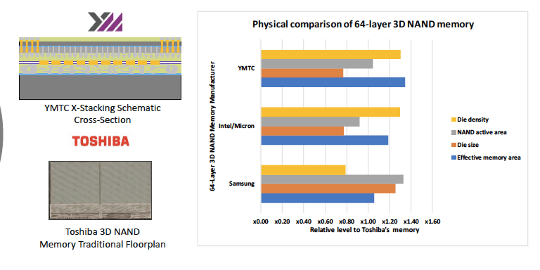
Hybrid bonding is proving to be a game-changer for memory, because it not only improves bit transfer rate but also the specification of memory with x-stacking of logic, noted Elisabeth. While hybrid bonding has been used for CMOS image sensor technology for some time, YMTC has the first memory product on the market using it (Figure 1).
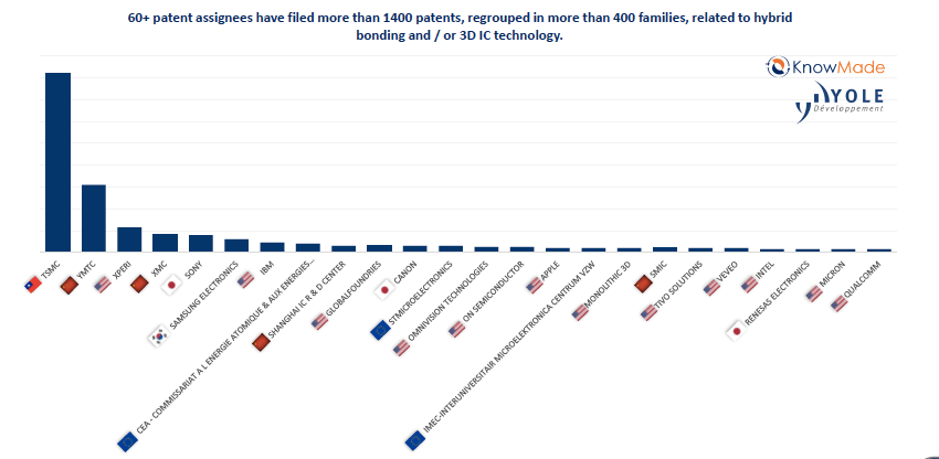
Leading companies (YMTC, Xperi, XMC, Sony, Samsung Electronics, and IBM) are prioritizing 3D IC and/or hybrid bonding IP strategy. Figure 2 shows the breakdown, but lumps hybrid bonding and 3D IC IP together, putting TSMC in the lead, and YMTC in second place, followed by Xperi. I’d like to see an analysis that focuses solely on hybrid bonding to see that breakdown (Figure 2).
The bottom line (and thank goodness for conclusion slides):
- 3D/2.5D packaging is an essential part of the semiconductor industry, extending Moore’s Law at the system level
- The value of 2.5D and 3D integration is its ability to accelerate 3D interconnect density.
- Cloud computing, networking, and high-performance computing are all experiencing a high adoption rate of 2.5D/3D system units
- Adoption in consumer devices, personal computing, and gaming is beginning, and the trend is expected to continue
- Future digital trends in end systems require a far more intelligent and therefore multifaceted devices. This leads to an intensive trend towards finer pitch and 3D/2.5D integration at the package level.
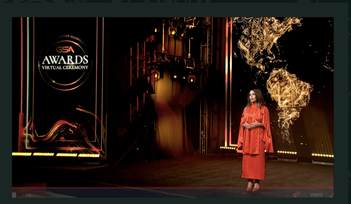
The GSA Awards
The GSA Awards ceremony offered all the pomp and circumstance of a Hollywood production, from the stylized video intros to the acceptance speeches, to Jody Shelton’s glamourous gowns (complete with a costume change.) All the glitz and glitter showed that this annual event draws the semiconductor industry elite.

Before the ceremony started, I spent some time in the networking rooms. Kudos to the GSA for finding Wonder Online Events, which created a much more interactive experience. It was my first time using the platform and I was impressed. I popped in to see my friends at ASE Group Global, and chatted briefly with Patricia McLeod, Eelco Bergman, and a few others, stopped at Marvell to see if I knew anyone (I didn’t – I am not part of the semiconductor elite) then meandered over to the GSA room, where it seemed most people were milling about.
Shelton, AMD’s Lisa Su, and a host of industry dignitaries delivered inspiring remarks. Shelton talked about GSA’s membership expansion to represent the broader industry involved in the digital economy including companies like Facebook, Ericsson, and Cisco; its Women’s Leadership Initiative, and commitment to all efforts related to diversity and inclusion, as well as climate change. Shelton noted China’s investment in AI, with 100 “unicorns” that are mostly AI startups, “Trillions of smart, always-connected devices will produce a payday for semiconductor devices,” she said. “5G will open new groundbreaking possibilities and has taken the market by a storm with Qualcomm at the center.”
Of all the awards presented, the most poignant and compelling to me was the Rising Woman of Influence Award, which this year was presented to Jaya Jagadish, Corporate Vice President, Silicon Design Engineering, AMD.
“There is no greater inspiration and motivation than being recognized and acknowledged by industry peers,” she said. “My words of advice to women trying to build a successful career: Don’t lose sight of your long-term career goals because of short term challenges. Play to your strengths. We will work together to build a more equitable semiconductor industry in the coming decade.”
While deeply honored to receive the awards, Jagadish said she looked forward to a future where there would be no need for a term as “women leaders” but just “leaders”, and no need for a special award category for women. Indeed, the GSA’s Dr. Morris Chang Exemplary Leadership Award has only ever been awarded to one woman – Dr. Lisa Su, CEO of AMD, in 2019.
The rest of this year’s award-winning companies can be found here.
As mentioned early, this was a lot of information for one day, and the SEMI Webinar message was far too important to bury at the end of this blog, so it got its own post here.

