

Several decades ago, Asia began its quest to be a reliable and cost-effective IC packaging, assembly, and test partner for low complexity ICs. Since then, Asia has proven itself as the world’s dominant wafer manufacturer and developer of process technologies, down to smallest feature sizes.
On August 4, 2020, I had the opportunity to join, together with about 150 US-based semiconductor experts, an International Semiconductor Executive Summit (ISES) webinar that demonstrated Asia’s current capabilities in advanced IC packaging and heterogeneous integration (HI), as outlined by executives from Samsung and Amkor.
Salah Nasri, Executive Managing Partner ISES, introduced ISES Global, the webinar’s agenda, presenters, and moderator: Dae-Woo Kim, Corporate VP, Head of Advanced Packaging Development Team at Samsung, and Mike Kelly, VP Advanced Package and Technology Integration at Amkor Technology were the presenters. Amy Leong, Chief Marketing Officer and Senior VP, Mergers & Acquisitions at FormFactor, moderated this webinar.
Samsung’s Advanced IC Packaging Capabilities
Dae-Woo Kim emphasized that as feature-size shrinking is getting more difficult and very costly, “More than Moore” (a.k.a. advanced IC packaging, multi-die packaging) is, in most cases, a better way of packing more functionality into an IC package and with it, continues growing opportunities for our industry. Kim sees the need for much higher bandwidth than single-die ICs on a printed circuit board can offer as a key reason for multi-die packaging. He showed examples for integrating multiple chiplets (a.k.a. bare dice) in a 2.5D IC and listed chiplets’ technical and business benefits, also applicable in wafer or panel-level packaging.
Kim explained Samsung’s hybrid bonding technology and its integrated stack capacitor (ISC), that reduces mid/high-frequency noise. Last, but not least, Kim addressed my favorite subject: die-package-board co-design. With the increasing complexity of multi-die IC packaging solutions, challenges like IR drop, supply noise, crosstalk, signal degradation, thermal-mechanical interactions, and other factors in a die-package-board assembly, need to be analyzed in context.
Amkor’s Advanced IC Packaging Capabilities
Mike Kelly presented a very visionary message and outlined the different requirements and trends in the mobility market, in the Internet of things (IoT)/consumer applications, automotive, and high-performance computing (HPC) and networking systems. For example, mobility devices demand 5G and a tiny form factor. IoT edge nodes need high levels of heterogeneous integration and ultra-low power designs. And for automotive, reliability is the dominant criterion. Data Centers need performance, very high levels of integration, and excellent heat management. These significantly different requirements, and frequent needs for customization of packaging solutions, confirm the importance of having clear hand-off criteria between customer and assembly partner and demand an excellent working relationship for successful cooperation.
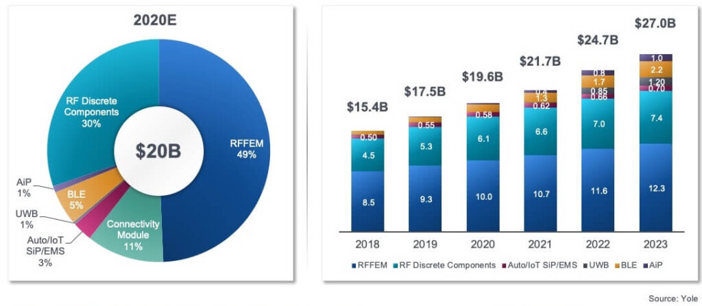
Kelly addressed another significant trend: The rapidly growing need for even more wireless communication links. In Figure 1 he explained the importance and growth of radiofrequency (RF) applications, showed the major RF building blocks – dominated by RF front-end modules (RFFEMs) and discrete components – as well as the variety of radios needed. Kelly emphasized that new materials with low dielectric loss angle/tangent (a.k.a. low insertion loss) are needed, to avoid/minimize self-heating and signal loss at 5G frequencies in the tens of GHz (FR 2 band / mm waves).
Besides RF challenges, Kelly talked about other major packaging requirements – like form factor reduction, high-power management, electrical-thermal-mechanical interactions – that challenge IC assembly houses and their suppliers. He said the future of packaging will mean solving those challenges by meeting innovation milestones including:
- Complex modular systems for miniaturization
- Electrical microsystems targeted to IoT, 5G and AI
- Electrically and mechanically advanced materials
- Power dissipation to andle higher power density
It is well known that artificial intelligence (AI) and machine learning (ML) are now deployed widely in data centers. Kelly stated that AI/ML functions are also needed in IoT edge nodes, to minimize local control systems’ response times, reduce network data traffic and power dissipation.

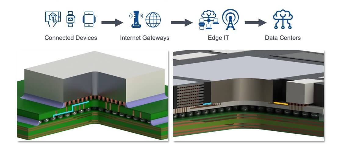
Big data capture, transfer, storage, and compute are today’s major challenges for the semiconductor industry in general, and specifically for IC packaging experts. Figure 2 shows a typical data flow from the edge node to the data center.
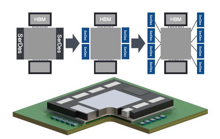
Another significant packaging trend: Customers want chiplets (a.k.a. bare dice, semiconductor IP building blocks in die-form), to reach far beyond the complexity limits of single-die SoCs, cut time to market, keep design risk manageable, and, most importantly, lower development and unit cost. Chiplets enable the integration of heterogeneous functions (logic, memories, analog, MEMS, etc.), each function manufactured in the most suitable and cost-effective process technology. Fig 3 shows a few of the benefits chiplets offer and how they enable them to integrate (sub)systems into an IC package.
To utilize the full value chiplets can offer, the connections between them, to the package and the board, need to minimize bit error rates, signal delays, and power dissipation (measured in pico-Joules per bit) as well as maximize bandwidth. Kelly showed how packaging experts have reduced bump heights/diameters from 70 / 70 µm to 10 / 15 µm and further to single digits, to meet these requirements. Amkor is also developing hybrid bonding techniques that will allow sub-micron pads and pitches in the future.
As emphasized above, IC packaging experts have to serve many different applications. To do so, Amkor has developed a broad range of packaging technologies – e.g. FC-MCM, 2.5D & TSV, HD Fan-out (SWIFT), and bridge & HDFO (S-Connect).
Personal Comments
Giving management-level overviews of Samsung’s and Amkor’s advanced packaging capabilities in less than 30 minutes each was clearly challenging. It obviously did not allow us to address other important topics, like progress in wafer-probe and test, package assembly design kit (P-ADK) development, nor materials characterization and modeling techniques.
Still, these brief presentations conveyed very clearly that a significant part of a system’s value creation is moving to advanced IC packaging. It enables heterogeneous integration, much smaller form-factors than single-die SoCs, mounted on PCBs can ever reach. Above all, smaller dimensions mean higher system performance, while reducing system power consumption and total system cost.


