
This week we continue our look at ECTC 2020.
imec and SPTS Collaborate on Nano-TSV Processes
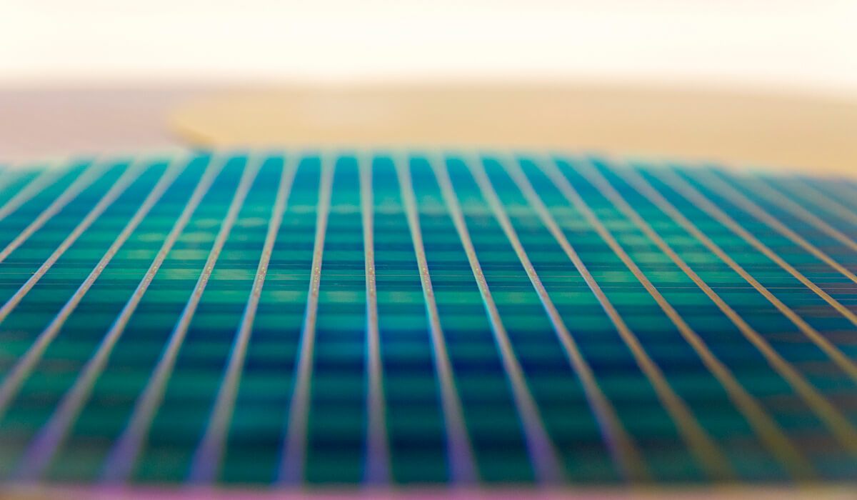
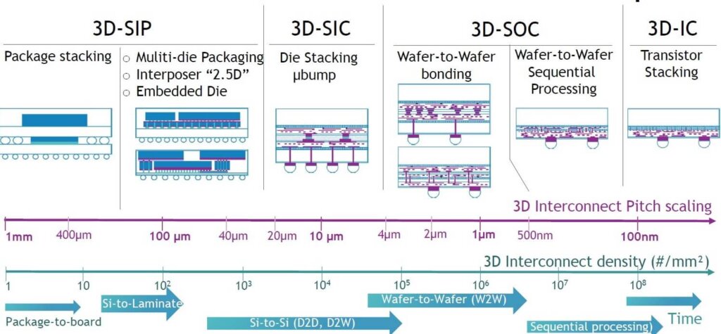
As part of our IFTLE theme of advanced packaging and interconnect going submicron, let’s look at the imec (long renowned for both their front end and back end work) presentation “Extreme Wafer Thinning and Nano-TSV Processing for 3D Heterogeneous Integration” by Anne Jourdain (Figure 1)
To reach sub 500nm interconnect pitches, they had to develop an extreme wafer thinning process with total thickness variation (TTV) thickness control over the full wafer and nano through-silicon via (nano-TSV) with a modified Bosch etching process. Using these processes, they have achieved 99% electrical yields between the front and backside of the devices.
The impact of the wafer-to-wafer bonding process on the TSV photolithography with respect to metal 1 must also be characterized.
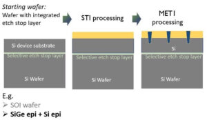
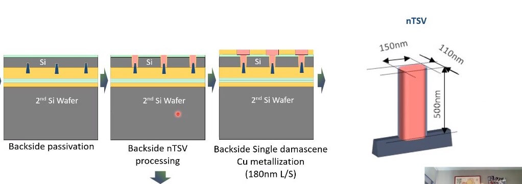
IMEC is looking into 0.7µm TSVs with 5µm depth. By further thinning the silicon from 500 to 300nm, the TSVs become nano TSVs with diameters of a few 100 nm. Such thinning requires etch-stop layers and several thinning processes in order to obtain the required dimensional control. The TSV process and the extreme wafer thinning process are shown below (Figure 2 and Figure 3).
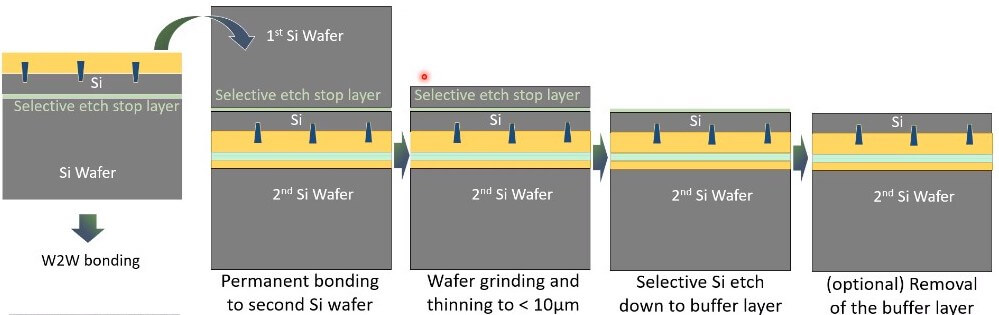
This requires grinding, dry etch, and wet-etch processes.
After wafer thinning to ~500nm they deposit a thin oxide layer (150nm of low-temperature oxide) as backside passivation. The nano-TSVs are aligned to the backside side metal. 150 x 110nm TSVs are filled with copper.
Nano- TSV alignment is a complex lithographic process. They have achieved 16nm (X) and 7nm (Y) overlay (Figure 4).
The Bosch process TSV-etch is more selective to oxide but the scalloping that shows up in micron-sized TSVs becomes unacceptable because the dimensions of the nano-TSVs are as small as the scallop dimensions (Figure 4).
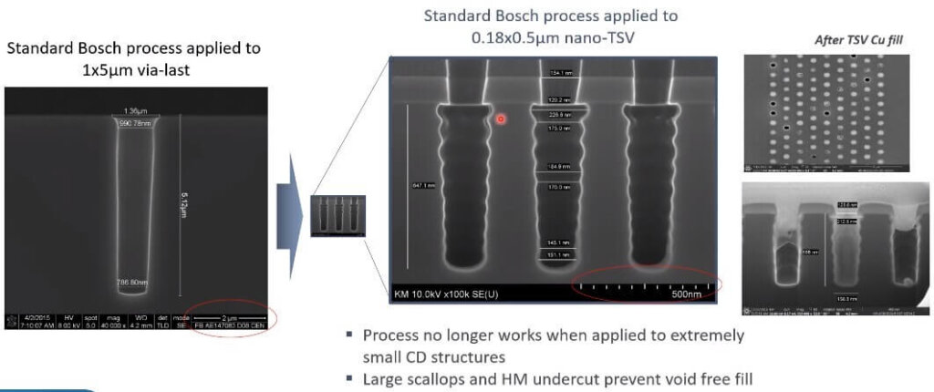
IMEC worked with SPTS to develop scallop-less nano-TSVs.
Functional electrical structures were measured and characterized, showing up to 99% electrical yielding connections between the front side and backside of the device wafers, and confirming a final backside-to-frontside overlay below 15nm.

Canon’s Panel Stepper for FO-PLP
Mori, of Canon, updated attendees on the company’s “Study of Submicron Patterning Exposure Tool for Fine 500mm Panel Size FO-PLP”. Interposers for multi-die FPGA modules are limited to 26 x 33mm reticle size. However advanced packaging is evolving into larger packages and finer redistribution layers (RDLs). It is thought that panel-level processing (PLP) advantages increase over wafer-level packaging (WLP) as package sizes increase.
- Challenges of fine-featured FO-PLP include:
- Exposure tool resolution enhancement
- High-resolution photoresist development
- Panel flatness improvement
- Large panel coating tool uniformity
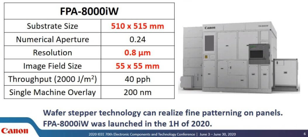
Canon’s sub-micron panel stepper is shown below with specs.
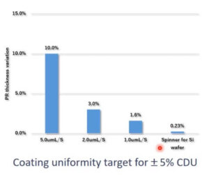
Resist coating uniformity has been modeled in Figure 7.
Whereas a 10% thickness uniformity is okay for a target of 5µm l/s, 1.6% uniformity is needed to achieve 1µm l/s. They modified resist to control evaporation of the solvent and achieved 1.7% thickness variation over the panel.
Further studies on plating uniformity, electric performance, and cost engineering are necessary to start high volume manufacturing of FOPLP.
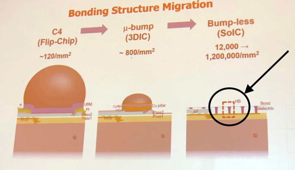
NOTE ON TSMC SoIC
After the publication of IFTLE 457 where I said that I had never see TSMC describe their SoIC process as being “hybrid bonding”, a reader who was at the IMAPS DPC in March wrote to indicate that Doug Yu’s presentation had a SoIC slide in it that had the initials HB pointing towards the bond. Since I was not there (avoiding the coronavirus) and Doug did not include his slides in the IMAPS download package, I certainly missed that. Below is a photo of the slide highlighting the HB from a reliable source. You have to look close, but it’s there:
For all the latest in Advanced Packaging stay linked to IFTLE……………………….


