
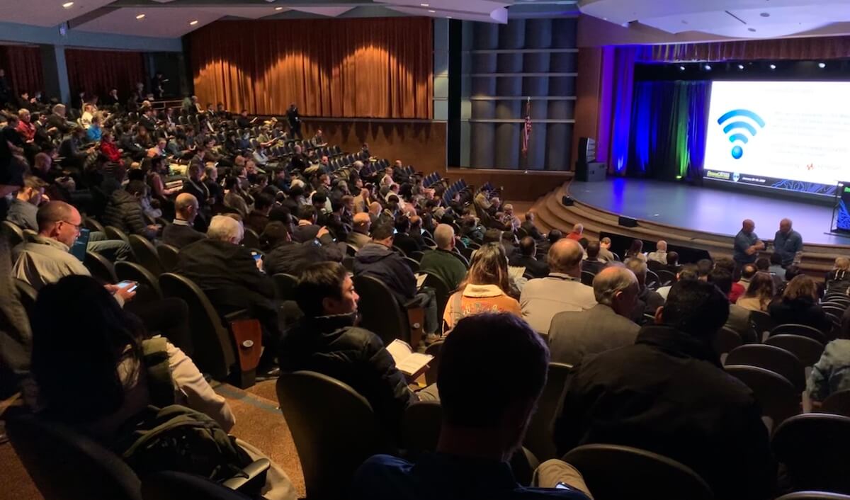
About 5000 attendees, as well as more than 200 exhibitors, took over the entire Santa Clara Convention Center from January 28 to 30, to hear the latest about IC, package and board innovations and to celebrate the 25th Anniversary of DesignCon. About 200 presenters conveyed very useful information in 14 parallel tracks and three keynotes. DesignCon 2020 was not only very educational but also a great physical exercise – my smartwatch counted more than 20,000 steps while I was rushing from session to session and visited exhibitors in the expo hall.
Data at the Speed of Light
The entire event demonstrated our customers’ hunger for Big Data, to feed AI algorithms. This hunger demands both high transmission and processing speeds as well as data security. In the first keynote, Chris Cole, VP Systems Engineering at Luminous Computing, addressed “The Future of Fiber Optic Communications.” He used examples from the evolution of Ethernet (IEEE 802.3) transmission speeds, starting with 10 Mb/s Ethernet connections, reaching their first million lines in 2008 and projected that 400 Gb/s with optical fiber will reach the first million links in 2023. Cole pointed out that many of these fibers are being used in parallel and gave “Data Transmission at the Speed of Light” a totally new meaning.
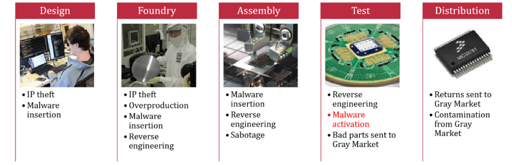
In Wednesday’s keynote, Warren Savage, Visiting Researcher at the Applied Laboratory for Intelligence and Security, University of Maryland/DARPA, focused on Design for Security. He explained how side-channel attacks allow hackers to listen to transmitted data, how reverse engineering can steal IP, how the insertion of malicious hardware into a design can compromise security and detailed vulnerabilities at every stage of the supply chain. He also explained blockchain technology and how it counteracts these threats (Figure 1).
In Thursday’s keynote Zaheer Ali, Senior Manager at the USRA Science and Mission Operations presented very impressive photos from outer space, taken with NASA’s Stratospheric Observatory for Infrared Astronomy (SOFIA) and other equipment. His slides confirmed in many ways that our planet is just a tiny part of the entire known universe.
Integration of Heterogeneous Functions in Multi-die ICs, SIPs, and Modules
My main reason for attending DesignCon was to see if and where multi-die IC technology is being developed and deployed. I got a resounding YES – multi-die ICs are now deployed widely. What impressed me most, was that many presenters who covered this topic are convinced that there is no better way to meet high-performance requirements at lower power, at this time.
I also need to point out: DesignCon 2020 showed that 2.5/3D-ICs are currently only used in very high-speed designs. Unit cost, as well as design, manufacturing and test challenges, are not yet addressed well enough to make multi-die ICs attractive for more cost-sensitive applications. Assembly & test experts at Amkor, ASE, JCET, other OSATs and foundries, like TSMC and Samsung, are developing lower-cost multi-die wafer/panel-level packaging solutions to serve also very cost-sensitive applications with multi-die ICs – stay tuned.
Highlights from Presentations in the 14 Application-specific Tracks and Company-sponsored Sessions
Knowing that 5G wireless technology is ramping up fast, I started DesignCon with a tutorial by Ben Jordan from Altium, titled “The Absolute Beginners Guide for RF & Microwave PCB Design”. I learned a lot about this challenging topic. His most useful points of advice for me were to study this book about transmission lines from Brian Wadell, get accurate formulas for stripline calculations from IPC-2252 and treat a connection to be a transmission line if it’s longer than 1/20th of the signal’s wavelength.
High-bandwidth memory, adjacent to a processor, on an interposer, is a very common multi-die configuration today. Billy Koo, from Samsung Foundry, compared the performance and power of LPDDR5, GDDR6, and HBM2 memories and explained for which applications each one is best suited. He also hinted that Samsung targets up to 6.4 Gb/sec signaling speed for HBM3. FYI, Samsung will present much more about their HBM capabilities and plans at ISSCC, to be held in San Francisco from February 16 to 20.
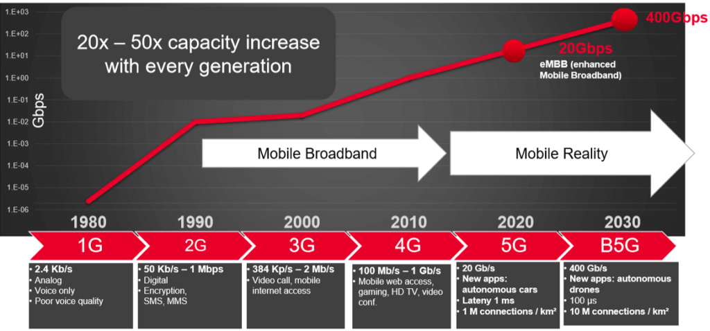
Beate Hoehne from Keysight in Germany, outlined decades of progress in wireless communication, comparing generations one to five in the slide below (Figure 2).
After discussing the wireless portion of a communication link – which is what our industry calls “the last mile” – Hoehne stepped systematically through the equipment and technologies needed to enable worldwide communication between humans and machines (Figure 3).
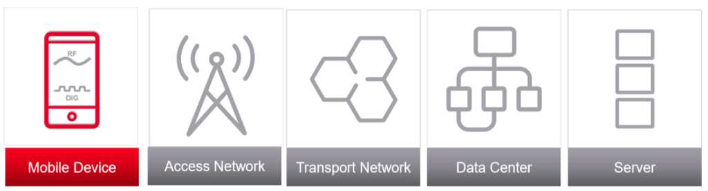
The above figure shows the uplink data flow. Imagine a mirror image of it for the downlink channel. Hoehne’s presentation addressed the need for access points – base stations and micro base stations, which receive sub 6GHz and mm-wave signals from wireless devices, hand-held or attached to machines. Regarding network, she mentioned that in 2018 there was 564 Million km of fiber installed worldwide, using quadrature modulation (QAM) to increase capacity. Data centers use up to 800 Gb/s transmission speeds, forward error correction (FEC), switch ASICs and convert electrical to optical signals. To improve server performance, hardware accelerators are used widely. In closing, Hoehne emphasized the importance of exhaustive testing and very high reliability for all components and systems in a network.

I also had opportunities to attend ANSYS and Cadence presentations, to learn about the latest EDA capabilities to guarantee power and signal integrity, reliability, as well as die/package/board design flows.
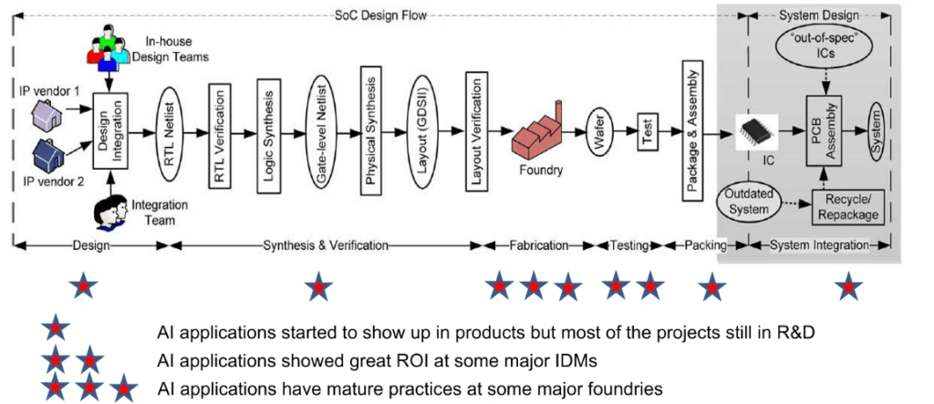
Last, but certainly not least, I want to mention the Si2 panel discussion in track 14: It addressed the question “Is a technology roadmap really needed for use of Artificial Intelligence and Machine Learning in EDA?” Si2’s Leigh Anne Clevenger organized, and John Ellis moderated this panel. Representatives from ANSYS, IBM, Intel, and NC State University explained the roadmap’s importance for design tools development. Even more significant, they emphasized the need for coordination, standards and security measures to make AI/ML work well across the entire semiconductor supply chain (Figure 4).
Summary and Personal Comments
Congratulations to the DesignCon management. Attracting 5000 attendees, 200 exhibitors and 200 very knowledgeable presenters is an impressive achievement. I look forward to another information-rich DesignCon in January 2021. Allow me to suggest an updated DesignCon tag line for 2021: “Where Die – Package – Board Meet”, because it’s widely recognized now that the needed multi-die integration increases the value contribution of IC packaging* to make electronic systems more competitive. If needed, I’ll be happy to introduce DesignCon organizers to key executives at IC packaging innovators, like ASE, Amkor, JCET, TSMC, Samsung and others, to win them as presenters and/or exhibitors for DesignCon 2021 and beyond.
Design productivity for cost-effective, low-power and reliable die/package/board/system solutions is important. That’s why I was very impressed that major design automation firms – specifically ANSYS, Autodesk, Cadence, Keysight, MathWorks, Mentor – A Siemens Business, and several smaller EDA vendors – were fully engaged at DesignCon 2020 as exhibitors and/or presenters.
*) If you want to know more about advanced IC packaging technologies and multi-die ICs, please review the Heterogeneous Integration Roadmap, even better, join us at the Heterogeneous Integration Roadmap 2-Day Symposium in San Jose/Milpitas, on February 20 and 21.
Thanks for reading…Herb


