
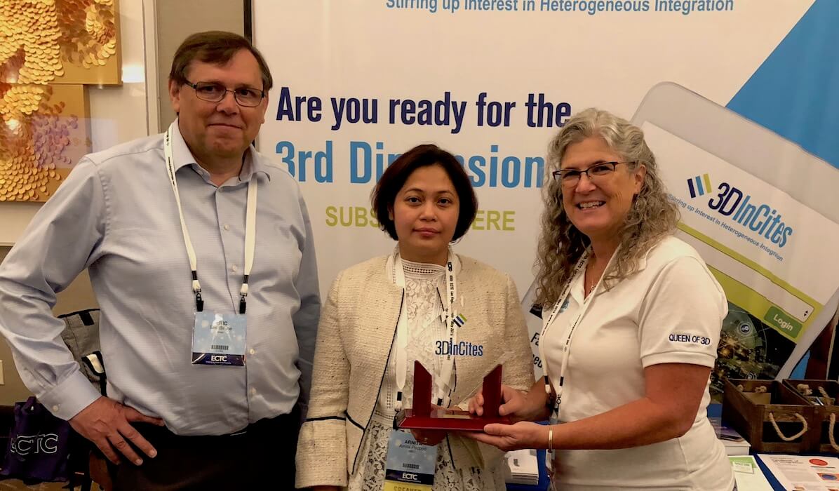
 3D InCites presented the 2019 process of the year award to Eric Beyne and Arnita Podpod of IMEC for their flip-chip on fan-out wafer-level package (FC on FOWLP) process that avoids the use of TSVs in active chips to achieve high-density packaging. Advanced packaging practitioners may have noticed the similarities to the Intel EMIB process (see IFTLE 400 “Intel Logic-Logic 3DIC and Chiplets are Finally Here”), and the Amkor through mold via process. Since several publications have now come out concerning this proposed process, we thought it was worth a closer look.
This concept basically uses a mold-first approach, where the dies are over-molded after the formation of the chip-to-chip interconnections. This way, contrary to the standard mold first approach (generally called “chips first”), chips are already interconnected before being shifted during the over-molding process.
By combining this approach with the development of novel mold materials, IMEC has demonstrated wafer bow below 500μm after molding on a silicon substrate and die shift as low as an average of 10μm across a 300mm wafer.
This has major implications on the processing of such over-molded substrates that could allow the use of more standard silicon back-end-of-line (BEOL) processing equipment and not require special dedicated equipment due to wafer bow.
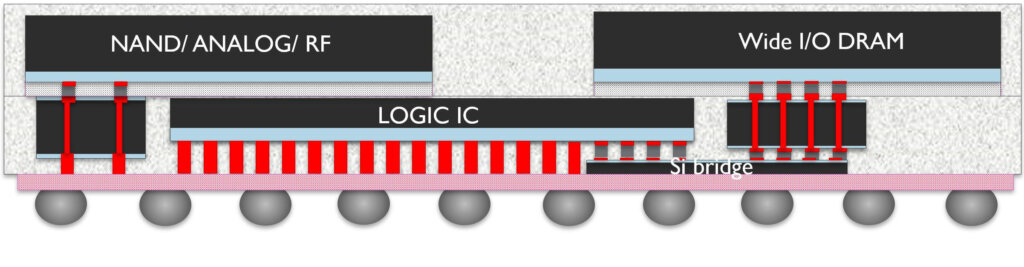
The test vehicle IMEC built, composed of dummy die (wide I/O DRAM, Flash memory, logic) along with through-package vias (TPV) and Si bridges were used to test the electrical continuity between the bump connections.
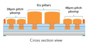
TPVs are Si dies with 5 x 50µm TSVs and bumps on 40µm pitch. The Si bridges are 20-30µm thick and 40μm pitch bumps are attached to the TPV side and the right side of the logic die. The 20μm pitch bumps are attached to the left side of the logic die. The 50um thick dummy memory die contain one metal layer and bumps with 40um pitch. The 55um thick dummy logic dies contain one metal layer, 50um tall Cu pillars, and bumps of 40μm pitch on the right side and 20μm pitch on the left side. The total thickness of the package body (excluding solder balls) is 0.3-0.4mm. (Figure 2).
In the first step of the assembly process flow shown in Figure 2 (1-4), the TPV and logic die are placed on a silicon carrier wafer with a temporary bonding layer. Next (5-6), the Si bridge (with 40µm and 20µm bump pitches) is attached using a thermocompression bonding (TCB) step. In this process step, bumps with 40µm pitch are attached to the through-package via side and to the left side of the logic die. The 20µm pitch bumps are attached to the right side of the logic die. In the next step (7), the wafer is over-molded by a liquid mold compound. Tests revealed a complete filling, even of the area under the bridge. Next (8), the Cu pillars are exposed by grinding – to connect with the redistribution layer later on. After flipping the thinned wafer to a second carrier and removal of the first carrier (9-11), the memory dies are assembled using flip-chip technology (12-13). A second wafer-level molding (14) and removal of the second carrier (15-16) complete the process flow. Continuity tests are performed In between process steps, to verify the electrical paths.
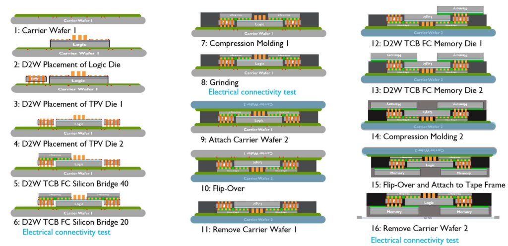
Figure 3 shows a cross-section after the 2nd mold operation.
To assess die tilting, TPV placement was done with placement forces of: 4.9N, 7.4N, 9.8N and 12.3N. Tilting of the die after placement was measured using a high resolution profilometer. They observed that, even for the largest placement force, tilting was limited to below 5µm which was low enough to maintain the connections.
A precise alignment step is needed to enable the subsequent 40µm and 20µm bump pitch stacking of the Si bridge. For example, to achieve the required 20µm bump pitch, a misalignment of max +/-3µm between the logic and through-package die can be tolerated. To reach this exceptionally small misalignment, the team incorporated alignment marks into the carrier and die designs. Logic dies were first aligned to the carrier. Next, through-package dies were placed, aligned to the carrier and to the logic dies. Finally, a high accuracy placement and stacking thermocompression bonding tool was used to attach the Si bridge.

During the subsequent molding process, the dies might still shift – thereby damaging or breaking the bump connections between through-package via and bridge, or between logic and bridge. The IMEC team ran electrical tests, before and after the molding. The tests revealed that the molding process did not affect the integrity of the connections.
The presence of Cu pillars on the logic dies make it difficult during pick and place step due to vacuum loss. A specifically designed soft collet was used to solve this issue.
This technology requires accurate placement of the logic and TPV dies followed by thermocompression bonding (TCB) of the bridge connector before wafer-level overmolding. The accurate placement was achieved by incorporating alignment marks into the carrier and die designs and the use of high accuracy placement & stacking TCB tool.
Another potential issue is incomplete mold underfill under the silicon bridge interconnect. Based on the SAM (acoustic) images and representative cross-sections, the area under the bridge can be completely filled with mold material. IMEC comments that “The mold process parameters have not been changed from baseline parameters” to do this, but have not yet shared exact conditions to achieve this complete MUF underfilling. IFTLE will be keeping an eye on this intriguing packaging concept.
For all the latest in Advanced Packaging stay linked to IFTLE……………………………


