


When we look back at the last 10 years, it’s really been a series of baby steps to move the commercialization of 3D integration technologies forward. There is no single pivotal event that catalyzed the 3D evolution. Like the Chinese philosopher, Lao Tzu said, “do the difficult things while they are easy and do the great things while they are small. A journey of a thousand miles begins with a single step.”
Our challenging journey of 3D integration has been marked by many incremental accomplishments and milestones. A few noteworthy events include the first commercialization of 2.5D FPGA integration by Xilinx and TSMC in 2011, mass production of high bandwidth memory (HBM) in 3D stacks by AMD and Hynix in 2015, and the latest Intel announcement of Foveros 3D chip stacking technologies in 2018.
One common driver behind these innovations is to leverage advanced packaging technologies to supplement the slowing of Moore’s law for transistor scaling. From a probing technology perspective, the adoption of advanced packaging (copper (Cu) pillar, TSV, etc.) has driven rapid pitch reduction and a corresponding density increase for probe cards. Over the last 10 years, the minimum grid-array probe pitch has reduced from 150µm to 40µm, while the total probes per card have increased from ~10K probes to over 100K probes. These trends have breached some interesting thresholds:
- The diameter of a probe becomes smaller than a human hair ~100µm, it is at or beyond the positioning accuracy of most human hands.
- The manual probe assembly (~1 min. per probe) will result in longer probe card assembly time than wafer fab cycle-time of ~45 days (65k mins).
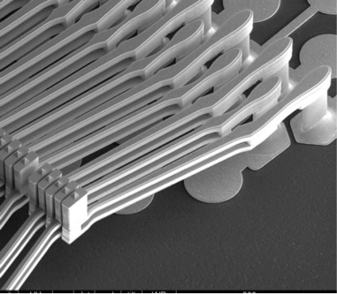
In 2013, FormFactor was the industry’s first to bring the automated vertical MEMS probe assembly capability to build fine-pitch, multi-site probe cards Today, we continue investing significantly in MEMS probe and automation capabilities and routinely build probe cards with probes as small as 20um, ~1/5 of a human-hair diameter. Our MEMS probe engineers humorously said, “our job is to split a hair daily!”
While the technical solutions for 3D and heterogeneous integration have been demonstrated, the commercial bottleneck remains. Today, the adoption of 3D integration is still limited to a few performance-hungry applications such as data center and artificial intelligence (AI), not widely used for consumer-driven mobile applications.

In the next 10 years, we need to drive a higher level of back-end manufacturing automation to reduce the total cost of the 3D stack. For example, many improvement opportunities exist in the areas of singulated die handling, testing, transporting, as well as process control software and data analytics, to advance the yield of the singulated thin-die and the ultimate stack.
My crystal ball sees a fully-automated and high-throughput die assembly and test floor at OSATs and foundries in the next 10 years, gradually moving away from wafer-based processing as the adoption of heterogeneous integrations increases.


