


![]() Packages and boards are playing an increasing role as a way to increase speed and density while reducing power and form factor of electronic systems. This is part of a trend called sometimes “more than Moore”, to refer to factors in addition to scaling ICs. Packages and boards both represent sizeable industries, even compared to the $300 billion semiconductor industry. Packaging is estimated to be an approximately $24 billion of revenue industry, while boards are estimated at approximately $60 billion of yearly revenue. This paper focuses on the simulation of the package-board system, which is becoming increasingly more complex and often requires solving the electromagnetic fields.
Packages and boards are playing an increasing role as a way to increase speed and density while reducing power and form factor of electronic systems. This is part of a trend called sometimes “more than Moore”, to refer to factors in addition to scaling ICs. Packages and boards both represent sizeable industries, even compared to the $300 billion semiconductor industry. Packaging is estimated to be an approximately $24 billion of revenue industry, while boards are estimated at approximately $60 billion of yearly revenue. This paper focuses on the simulation of the package-board system, which is becoming increasingly more complex and often requires solving the electromagnetic fields.
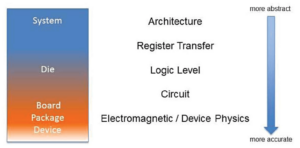 Electromagnetic simulation consists of solving Maxwell’s equations to calculate the electric and magnetic fields. In electronic systems, electromagnetic simulation is used to characterize the behavior of interconnect accurately. Stated in a simplified way, this becomes necessary when a signal travels a distance comparable to its wavelength and needs to be modeled as a wave. In practice, electromagnetic simulation is used for “fast” packages and boards, less frequently for dies because they are smaller. For example, at 1 GHz, the wavelength in air (very similar to vacuum) is 30 cm or about one foot, so signals that travel several centimeters require electromagnetic simulation; packages and boards exhibit these dimensions.


