
Last week, September 13 to be exact, TSMC held its Open Innovation Forum (OIP 2017) Symposium at the Santa Clara Convention Center. Before getting into product and market details, allow me to share some of my general impression of this, as usual, very well-organized event.
After several decades of experience with alliance management and ecosystem building, I see TSMC as the master of these disciplines. Supported by TSMC’s design enablement team headed by Cliff Hou, 50 OIP partners exhibited their EDA, IP and services strengths to complement TSMC’s manufacturing prowess in front of mutual customers. In addition, 33 of these OIP partners presented their capabilities, often together with a mutual customer. I honestly don’t know a better way than these annual OIP events to demonstrate the fruits of 30 years of hard work and many smart and strategic TSMC moves.
A few more important points became clear to me at OIP 2017: TSMC focuses on very high growth market segments, (e.g.high performance computing (HPC), automotive, 5G, and internet of things (IoT), offers silicon AND packaging capabilities, recommends reference design flows, even offers utilities to port designs from one process technology to another. Observing all these, phrases like “one-stop shopping”, “complete products”, and “value-added solutions” come to my mind.
Let’s talk about some other highlights of this OIP Symposium:
David Keller, President of TSMC North America since June 2017, welcomed all the partners and many mutual customers, then introduced four of our industry’s most accomplished executives: Aart de Geus (Synopsys), Anirud Devgan(Cadence), Wally Rhines (Mentor) and TSMC’s own Cliff Hou.
De Geus congratulated TSMC on being 30 years young, the same age as Synopsys. Then he walked through these 30 years, from kindergarten to college graduation and talked about several joint key milestones on the way. I was waiting in vain for de Geus to mention that I was the junior high/middle school teacher who introduced these two companies in 1998, when they were about 11 years old and very much in need of learning about each other. but this is not the place to trade high school stories…
Anirud Devgan highlighted the market’s need for system-design solutions and reasoned how important Cadence’s IC packaging design tools are becoming on the way to system-level integration.
Wally Rhines also praised TSMC’s excellent cooperation for improving silicon and package CO-design solutions, such as Mentor’s Calibre 3D Stack.
Cliff Hou started his presentation with a statement I really liked to hear: “3D-IC opportunities are growing rapidly and get TSMC’s full attention!” He announced new members for TSMC’s integrated fan-out (InFO) family of packages and mentioned that their chip-on-wafer-on-substrate (CoWoS) technology is becoming more and more popular. I hope, when Hou very briefly mentioned that he sees already opportunities for “wafer-stacking”, he really referred to vertical stacking on the wafer-level and market requirements for true 3D-ICs.
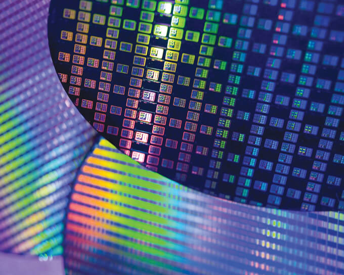
Then Hou announced that the N7 qualification is done and risk production is starting for up to 10 designs, by year-end. TSMC is already working on the N7+ node, with 8-10% better speed and 15 to 20% lower power. He also compared TSMC’s 12 FFC area, speed and power with their 16 FFC technology and stated 18%, 5% and 14% respective improvements. Hou also emphasized that TSMC offers a planar 22 ultra-low leakage (ULL) process for 0.8V and even 0.7V supply.
Last, but certainly not least, Hou talked about their cooperation with ARM to apply machine learning (ML) to IC design and mentioned that they currently achieve 8 – 12% performance gains by applying ML.

After the morning break and all afternoon, many OIP partners got the opportunity to outline how they complement TSMC’s many strengths. In three parallel sessions – EDA, IP, EDA/IP/Services Track – they presented their capabilities and described how, together with TSMC, they have developed solutions for customers. In addition to talking with many of the exhibitors on the floor, I had time to attend several of these impressive presentations:
- Sofics 25 – 56 Gbps silicon photonics I/Os for 28 nm CMOS
- Mentor’s enhanced Calibre smart-fill methodology
- Open Silicon’s HBM2 IP subsystem
- Kilopass’ OTP NVM solution for TSMC’s advanced nodes for automotive
- Flex Logix’s integration and validation of embedded FPGA configurations
- Mentor’s mixed-signal parasitic extraction flow for TSMC’s N16 process
- Analog Bit’s High Rel IP for automotive and data centers
- Cadence’s system planning solutions for CoWoS and InFO technologies
Every attendee got a handout, containing most slides of the partners’ presentations. If you want to know more about the above-listed capabilities and others, not mentioned here, please contact TSMC’s OIP partners.
What’s next?
Thursday and Friday of this week (9/21 & 22) I’ll be managing part of EDPS 2017. It will be held at SEMI’s new Headquarter in Milpitas, Silicon Valley. We’ll bring EDA, Design AND manufacturing experts together and talk about how ML can improve the cooperation within and between these camps.
On Wednesday, October 4, Mentor – A SIEMENS Business, will hold in Newport Beach, CA, an Advanced Advanced IC Packaging seminar. Jan Vardaman from TechSearch, Mentor’s Kevin Rinebold and I will be presenting.
On October 9 – 12 IMAPS will hold its 50th Anniversary Symposium on Microelectronics in Raleigh, NC. Many packaging and assembly experts will present. My part will focus on the importance of EcoSystem building. Exactly what TSMC demonstrated on September 13.
Looking forward to meeting you at some or all of these events! ~ Herb


