

I am convinced that increasing device complexity, higher quality requirements (e.g. automotive and medical), as well as the need for faster production ramp-ups, will force our industry to pay even more attention to design-in quality, expand self-test, even add redundancy to control logic and interconnects. In addition, wafer-probe and final test need to be expanded. Therefore, attending the Test Vision 20/20 Workshop on Wednesday morning and Thursday morning during SEMICON West 2017 had a high priority for me. This workshop taught me several key points.
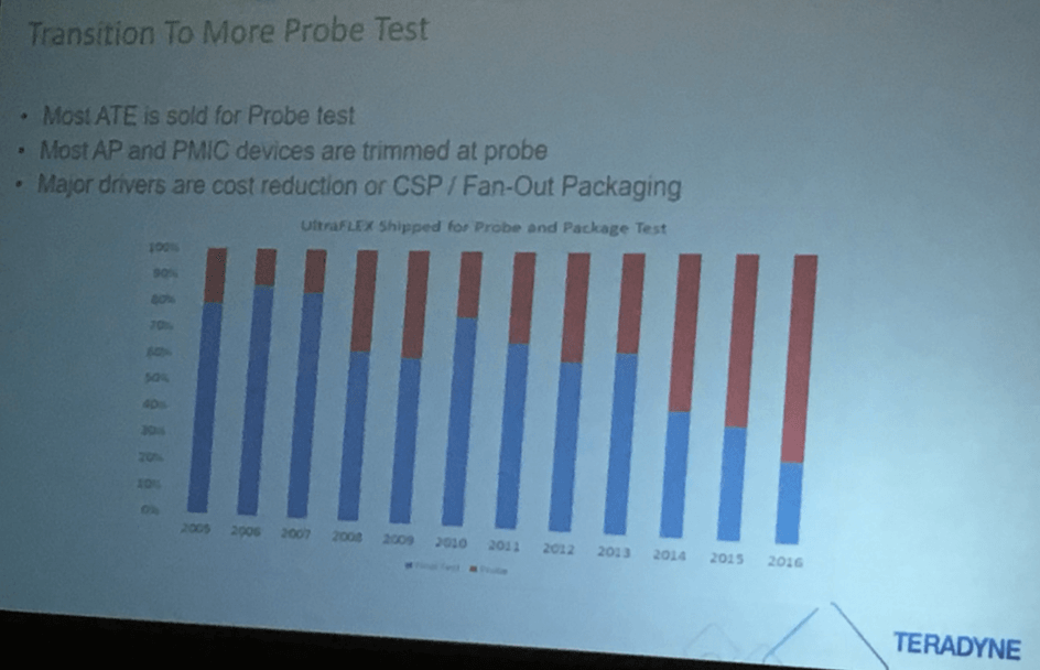
As wafer-level packaging technologies, including multi-die ICs, raise the importance of known good die (KGD), the development efforts in design and test are responding accordingly by expanding wafer probe. Greg Smith, President of Teradyne’s Test Division, conveyed the shift with this slide.
- A more significant trend is the need for system level test (SLT). As the integration levels continue to increase, and more heterogeneous functions are packed into an IC package, testing such an IC reaches typical board if not system-level complexity. To steadily improve yield and perform failure analysis quickly, traceability of every component in such an advanced package becomes a very important requirement.
- Speaking about SLT: Antennas are also becoming important parts of a system-in-package. Especially I/O edge nodes transmit their data wirelessly and require antennas to be part of an advanced IC package. It’s immediately obvious that, e.g., the traditional cost reduction strategy – multi-site test – can’t be applied for this kind of IC tests.
- The ability to trim passives, program a security code into a device, test across a very wide range of operating conditions – at the finished part and at the wafer-level – introduce new challenges for test experts.
Advanced Packaging
After focusing for almost 10 years on 2.5/3D-ICs, the advanced packaging sessions on Wednesday were another must see for me. ON Semiconductor’s Mike Seddon, Principle MTS in Corporate R&D, conveyed in the slide below how complex and multidimensional – from a process, voltage, current and temperature perspective – today’s requirements are.
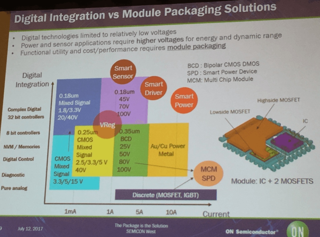
Seddon also conveyed two other interesting data points: In 2016 there were 88 million cars sold worldwide. Hybrid and fully electric cars need MOSFETs that can switch 100+ Amps at up to 650 Volts.
Cisco’s Nan Wang, Senior Director Q&A, said that bandwidth requirements in networking force a shift from traditional busses to crossbars on a chip. He highlighted that 2.5D and 3D ICs (HBMs) enable new architectures, allowing the mix of electrical and optical functions and the combination of NPUs in advanced feature sizes with SERDES dies, implemented in much larger geometries.
Key challenges with 2.5D/3D ICs for Cisco are cost-effective thermal management, alignment errors in silicon photonics assembly, test methodologies and in-field repair, time to market, and last, but not least, overall supply chain management.
Xin Wu, VP silicon technology at Xilinx, the first company to introduce a multi-die IC more than 10 years ago, stated that Xilinx’ complex FPGAs offer redundancy and self-repair and briefly talked about their rich history.
Boeing’s technical fellow, Tim Lee, informed us about his 5G-focused work at IEEE and projected a broad market acceptance for this high bandwidth wireless communications standard. He emphasized the importance of integrating antennas in advanced IC packages and projected that glass will replace silicon interposers in 5G applications because permittivity of silicon doesn’t allow the high operating frequencies of 5G devices.
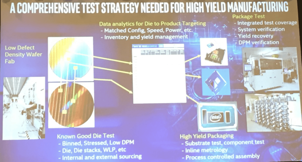
Intel’s Corporate VP and GM, Babak Sabi, was the first speaker in the Wednesday afternoon session. He conveyed his high-level perspective and stressed that a comprehensive test strategy – including the entire supply chain – is needed to achieve high yields in a volume production environment.
No doubt, this is a very critical topic for the continued success of high complexity and high-performance ICs. That’s why I want to highlight at this point an opportunity to meet many supply chain experts, from EDA to final test for HVM at SEMI’s Headquarters in Milpitas on September 21 and 22. SEMI is going to host the Electronic Design Process Symposium (EDPS) . Presenters from EDA and IC design companies as well as assembly and test experts will address exactly this topic during the 1 1/2day conference. In addition, machine learning (ML) experts will present ideas on how to use these rapidly emerging capabilities to analyze big test data quickly and engage the relevant supply chain partners right away in failure analysis and yield improvement measures.
ASE’s CP Hung, VP Corporate R&D (who will also present at EDPS!) showed the company’s broad portfolio of advanced packages. He confirmed the need for SLT test and other test requirements outlined above.
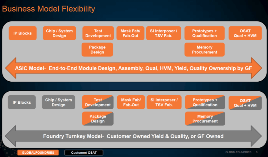
David McCann, VP Packaging R&D at Globalfoundries, explained their cooperation strategy with OSATs and emphasized the importance of a well-structured supply chain and the benefits of having one consolidator for complex multi-die ICs. The slide below shows Globalfoundries’ main business models and their responsibilities sharing strategy.

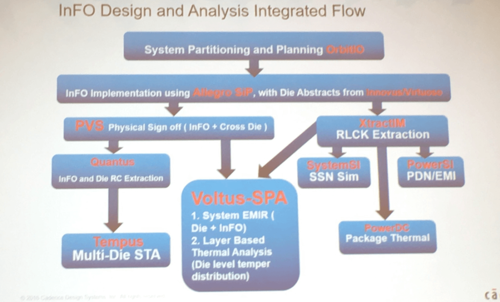
The only EDA presentation I could attend was Brandon Wang’s message about Cadence’s design support for multi-die ICs. He showed and explained how to use their different families of design tools to plan, design and verify multi-die ICs in advanced packages. As an example, for a proven design flow, Wang showed the TSMC reference flow for InFO (Integrated Fan-Out) packages, that are in use in Apple’s A10 processor in every iPhone 7.
After most of the previous speakers exceeded their time budget, Bill Bottoms’, the Chairman of 3MTS, had only less than 10 minutes left for his presentation. It was enough for Bottoms to convey and explain his key message: “The path to success is no longer shrinking of feature sizes.” That’s why the ITRS working group efforts had been terminated mid of last year and the HIR group had been formed.
The 411 on 5G
On Thursday morning, I joined the 5G session to learn how the output of our industry, the semiconductor components, are and will be used in this very promising application. Sree Koratala, VP and Head of Technology at Ericsson, projected very encouraging growth for 5G and showed that the number of today’s single digit Billions of 4G/LTE devices will be dwarfed in several years by the number of 5G nodes.
She also explained that it takes a team of companies, in this case namely Ericsson / GE / Honeywell / Intel as well as UC Berkeley, to drive the roll-out of this high-speed wireless technology.
Cedric Delos from CEA Leti explained that 5G’s higher bandwidth needs more relay cells than today’s 4G/LTE technology. With it the “backhauling” (= connecting the many small cells to the internet) becomes a significant challenge … and a great opportunity for more silicon. Representing CEA Leti, the inventors of high-quality SOI substrates, Delos, of course, pointed out that SOI is well suited for these high-speed applications, even for embedding antennas on silicon.
Jag Bolaria, an analyst at the Linley Group, outlined several of their projections for increasing compute power with GPUs and FPGAs, how ML and eventually AI will change our lives, why much more data storage will be needed, why and how photonics will replace copper connection.
Intel’s Robert Blum, Director of Strategic Marketing, also highlighted that optical connections are essential for coping with the vast amounts of data to be transferred in future. He explained that an Indium-Phosphide die-let (= die-level IP building block) mounted on top of a silicon logic die, can significantly improve performance per Watt.
Economics of Density Scaling
Because it helps my role as multi-die IC supporter to look occasionally across the fence into the world of feature size scaling, I attended “Economics of Density Scaling” on Thursday afternoon.
Diedrik Verkest from imec, Larry Clevenger from IBM, Jamil Kawa from Synopsys, Mark Bohr from Intel, Mike Chudzik from AMAT and Gurvinder Singh from Rudolph Technologies presented how they are achieving very impressive results in a world of mid and low single digit feature sizes, but I had to wait in vain for specific examples how the economics of single digit features rewarded the IC designers for their enormous efforts. I agree: Moore’s Law it not dead, but suggest replacing “feature size scaling” with “system scaling” for the overwhelming majority of design starts.
In summary, a very impressive trade show, spanning across the entire semiconductor supply chain. The many parallel tracks and the opportunities to meet with exhibitors, allowed me to only enjoy a small part of this very well organized and impressive trade show. (If you missed part 1 of my SEMICON West 2017 coverage, you can find it here. ~ Herb


Great summary Herb!