
Stress Test, noun: “A test designed to assess how well a system functions when subjected to greater than normal amounts of stress or pressure.” [Source: Oxford Dictionaries.]
The 27th annual SEMI Advanced Semiconductor Manufacturing Conference was off to the races the week of 16 May 2016 in charming Saratoga Springs, NY, for a three-day meet of invited keynote talks, technical papers, posters, a tutorial on Xtreme Transistors, a panel discussion, and more.
In terms of statistics, ASMC 2016 featured 353 registrants (a capacity crowd), 96 technical papers, 8 invited speakers, a tutorial led by 1 brilliant MIT professor, and zero reported frowns.
Other statistics: from Saratoga Springs it’s 12 miles to GLOBALFOUNDRIES Fab 8 in Malta, NY; 35 miles to SUNY Polytechnic CNSE in Albany; 90 miles to the Marcy Nanocenter, where ams is breaking ground on their new wafer fab; 120 miles to the GLOBALFOUNDRIES / IBM site in Burlington, VT, and 130 miles to their Fishkill, NY, site. All major semiconductor capital equipment suppliers have offices in the region, and academia is well-represented by the aforementioned SUNY Polytechnic CNSE, RPI, SUNY Polytechnic Institute Marcy, and other favorites.
In other words, this part of New York State is a hotbed of semiconductor manufacturing.
What better place to network with industry peers and share tradecraft on new, and best-method, semiconductor manufacturing practices and concepts vital to continued progress in the field?
If there is I don’t know of it.
Jonathan Davis, SEMI, has two pieces out on the ASMC 2016 Day One and Day Two Keynotes. See “IBM Keynoter Outlines Disruptive Economy of Things at SEMI’s ASMC 2016,” and “Driving the Digital Age of Manufacturing ─ GE Keynote at SEMI’s ASMC 2016,” for his very well-written takes on the remarks from these two very major players.
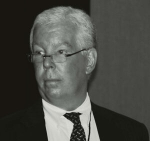
And also from SEMI, about the third keynote speaker, Robert Maire, we read “Maire … discussed factors driving M&A in the semiconductor industry during the final session of ASMC 2016 … Maire cited a slowing of organic growth, and motivations toward geographic and product diversification as trends driving general industry consolidation. … He said that companies can spend hundreds of millions on R&D, but the result takes years to materialize. They find acquisitions can be productive much more quickly. … He thinks that the ‘easy’ consolidation has happened first, but a few good targets in yield management, back-end packaging, and Japanese equipment sectors remain. … Maire also says that the Lam/KLA deal will likely still occur, but the companies may have to make concessions to Department of Justice regulators that may reduce its attractiveness.” (Oh, and he also said that the recent Chinese $23B bid for Micron Technology was straight from the Donald Trump playbook – good only for the PR value.)
 About that Silicon Stress Test: I wasn’t just enjoying ASMC 2016 as an attendee, I was there working, too, as the panel discussion moderator for “Moore’s Law Wall vs. Moore’s Wallet, and Where Do We Grow from Here?”
The background: 2015 was a year that saw the semiconductor industry expend nearly equal money on M&A activities as it did on Research, Development, and CAPEX combined.
$110B (M&A) to $120B ($56B R&D + $64B CAPEX).
Moore’s wallet was pulled out just about as much for acquisitions as it was for technological aspirations.
Students of business history may recognize that the semiconductor industry is at a place in its maturity “Characterized by mega-deals and large-scale consolidation plays. The goal now is to emerge as one of the small number of global industry powerhouses.”
We are following the path of Aircraft OEMs, and maybe also Brewers, where executing on consolidation strategies for the business becomes as important as making improvements to the products.
Our industry continues to face challenges of physics, in EUV Lithography; ALD and ALE; and in XTreme transistor architectures, that will only be surmounted by applying the combined, dedicated efforts of devoted scientists and engineers worldwide together with applications of money sufficient to fund those efforts.

The ASMC 2016 Panel Discussion featured four panelists, industry veterans representing the device maker, supplier, and customer communities, who offered their take on Moore’s Law versus Moore’s Wallet, and where do we grow from here.
In the brief amount of time allotted the panelists for their prepared remarks before going to interaction with the audience, we heard Dave Bloss, VP Technology Manufacturing Group, Intel, stress-testing the hypothesis that advancing semiconductor processing technology actually lowers overall manufacturing costs when considered over a long horizon. Unit demands would have to decrease significantly, on the order of 25%, to offset the positive aspects of scaling; R&D costs per device generation would have to almost double to have a net negative effect; and it is only a third horseman, poorer Cost per Transistor scaling, that could challenge in any kind of serious way, the overall economic benefits of investing in advanced semiconductor manufacturing processes.
Dr. Andreas Knorr, Director of Technology Research, GLOBALFOUNDRIES, managed to convince us in his remarks that, in order to address the observation that die cost did not necessarily decrease in tandem with pitch scaling, starting at the 32nm – 22nm process node transition, Design Technology co-Optimization becomes essential as we wait for the introduction of commercial EUV lithography.
 Patrick Martin, Head of Field Technology, Transistor and Interconnect, Applied Materials, is certain that with better interface control (at the atomic level), with better film deposition control (lattice matching), with better pattern definition (directed self-assembly), and with better architectures, including 3D architectures, Moore’s Law is sound at 7nm, with disruptive technologies waiting in the wings.
And the message from Bill Miller, Vice President, Engineering, Qualcomm, will be music to all 3D InCites readers: the speed bump we may be seeing for Moore’s Law, the one causing us all that stress, is going to be made better by the industry featuring more … SiP and Heterogeneous Integration.
Why, Bill?
To start, with SiP and heterointegration it’s possible to use the best process node for each/all of the various, integrated, applications, rather than having to choose one process node that gets the job done for a function while not being best for another; SiP / heterointegration also offers rapid time-to-development, possible reuse of system software, and it offers form factor size reductions for real system applications.
When Qualcomm, a $25B+ annual revenue (FY2015) company, supports SiP / heterogeneous integration as the way forward, your heterointegration ship came in, baby, as did your horse, if you were indeed backing heterointegration technology, as you know we’ve been doing here at 3D+ ever since we started this blog.
We’ll look at the ASMC 2016 3D / TSV papers in a second installment, soon. Right after we enjoy our winnings.
From Santa Clara, CA, thanks for reading. ~PFW


