

Isn’t it interesting how different people attending the same event can come away with different perspectives? I attended last week’s 3D Architectures for Semiconductor Integration and Packaging (3D ASIP 2014), and came away feeling euphoric about what the 3D industry has achieved since last 3D ASIP, and all its promise for the future. After following the technology progress and believing in it for so long, we can finally say it has arrived! So far I’ve posted two blog entries based on the event – one was a recap of the pre-conference symposium that took place on Wednesday, December 10, 2015, and the other talked about how 3D integration technologies are expected to enable the Internet of Things (IoT), and how perhaps we should define success by the opportunities 3D enables rather than whether the cost will ever be low enough for consumer applications.
Since I posted those, I’ve read three other actual accounts of the event, as well as one post that references it, and discovered that reactions range from overly enthusiastic (that would be me) to cautiously optimistic, to downright skeptical. Admittedly, I’ve always been a big proponent of 3D integration technologies, and as such tend to be hyper-optimistic about it. But I’m still taken aback whenever I read something written by another industry journalist that has any sort of negative spin to it. I get almost indignant. “Come on people! We’re there. Let’s celebrate! The rest will take care of itself!”
A post by SemiMD’s Jeff Dorsch, was probably the most optimistic account of the three (next to mine). Dorsch’s executive summary of the event paints a balanced picture of where we are, as he shared snippets of some of the key presentations, highlighting both the year’s big wins and the hurdles for the next phase. Overall, Dorsch summed up the industry’s status in two phrases: “It’s complicated” and “It’s promising.” And he’s spot on with those. It’s also going to be worth the effort, as Phil Garrou pointed out: “Anyone not now in the game will lose the position on the leading edge!”
In his post on SemiWiki, 3D: The State of the State, Paul McLellen first points out that 3D and (interposer) devices are still too expensive for most applications. But then he delves deeper into it and admits there are “some pretty high profile 3D things happening.” He goes on to talk about all the various products in the wings, and declares 2015 “the Year of 3D” followed by the disclaimer that its only in high priced items for now. By the time I reach the end of his post I am heartened. He’s a believer!
But then in the next day’s post, titled, Will 3D ICs ever be Cheap Enough for High Volume Products?” focused on Chet Palesko’s (Savansys) presentation of the same title, he put more emphasis Palesko’s cost analysis, which yes, clearly shows that 3D ICs will likely never be as cheap as the incumbent technologies like wire bond and flip chip, and additionally, that Si interposer-based solutions are even more pricey than 3D ICS. But as Juergen Wolf, IZM-ASSID pointed out to me, you can’t really even cost-compare 3D ICs with Si-interposer solutions because that would be like “comparing apples to oranges.”
Palesko’s REAL point, (and McLellen does get to it by the end) is that the question we should be asking is not will 3D IC ever be as cheap enough for high volume products, but “Will the markets that require 3DIC grow fast enough to drive volume manufacturing?”
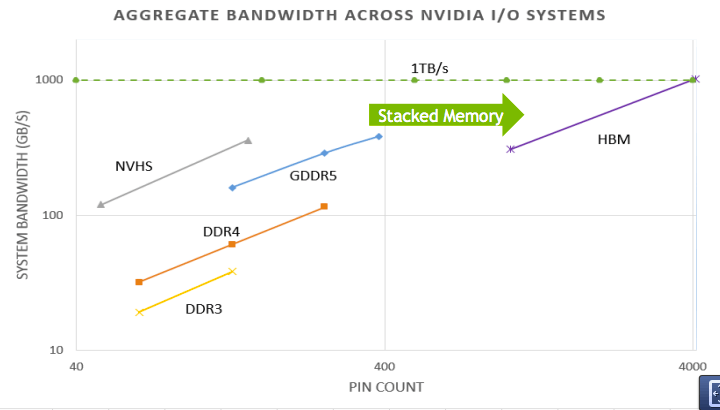
As I mentioned in a post earlier this week, Palesko said that like flip chip, 3D IC will likely always be a choice of last resort, but that doesn’t mean it won’t be successful. I would argue further that we shouldn’t refer to the 3D ICs as the choice of last resort, but as the choice of only resort, which means that really when it comes down to meeting the memory density and bandwidth requirements (such as the 1TB required for nVidia’s next-gen GPU) 3D ICs are the only way to do it (Figure 1). In that case, the technologies Palesko and McLellen describe as alternative technologies ( FOWLP, PoP, embedded die, etc) while albeit innovative solutions, are still no match for 3D ICs. It’s more likely that they will fulfill the needs of the high volume consumer products, while 3D ICs are busy taking on the high performance computing world, which, by the way, promises to grow quite substantially and could create a market for volume products of its own.

I was most surprised to read the title of Ann Steffora Mutschler post on SemiEngineering, Is The Stacked Die Ecosystem Stagnating? not to mention the opening line, “It is now widely agreed that not much has been happening in terms of adoption for 2.5D interposer and 3D ICs.” What??? Where have you been? Certainly not at the 3D ASIP Conference last week! Although she references 3D ASIP in this post, she couldn’t have attended it at all, because otherwise she would have had a different opinion altogether. She downplays the importance of memory stack product introductions, even while following it with a quote from Herb Reiter, who says “This is very essential step forward for the value proposition of 3D ICs because these memory cubes are, of course, 3D ICs.” Reiter not only attended ASIP but organized its Pathfinding panel discussion and Pre-conference Symposium on interposer/3DIC Design Tools and Flows.
Additionally, Mutschler mentions Intel’s silicon bridge technology, which Mark Bohr describes as a cheaper alternative to Si interposers. But she neglected to mention that Intel is implementing 3D stacked memory from Micron in its Xeon Phi processor for HPC.
While Mutschler’ s post does confirm manufacturing readiness, the skepticism she portrays from the design community is palpable. Its too bad none of the individuals (except Reiter) she interviewed attended 3D ASIP, not even its Design Tools and Flows Symposium, because if they had, they might have been enlightened.
“The people who are making things and the people who are designing things are not exclusive from each other,” said John Lannon, RTI, during his 3D ASIP presentation. “They need to be talking to each other.” The question posed by Jan Vardaman, Techsearch International, during the Pathfinding Panel was, “How do we get designers in the room to understand what the options are?” And by that I, don’t think she wasn’t referring to the designers actually in the room, because I could count them on one hand. What she meant was, how do we get designers into the room, so that they can understand what the options are? Maybe next year, the design community will take the hint and join in the dialogue. Because far from stagnating, this ecosystem is ramped and ready to roll. ~ F.v.T.


