
What with all the commotion about 3D NAND and the accompanying cyberspace chorus, you would surely be forgiven in thinking that its appearance was close at hand. So, the outlook for 3D NAND progress in 2014 should be fairly rosy then? Well, for the 3D NAND approaches touted so far, I beg to differ.
I foresee in 2014 the enthusiasm for these 3-D NAND approaches being gradually tempered by the main manufacturers. Nothing of course along the lines of “it won’t work” but rather it will take “longer”. In fact, this readjustment has already begun, as reported from a 3D NAND discussion forum at the International Electron Devices Meeting in Washington D.C. on December 10th. “Not all end markets will need 3D NAND” was an interesting admission.
Don’t get me wrong. I believe 3-D Flash is coming. Indeed, so much so that I’ve devoted the last 13 years working on it with the last 8 in my own company. And this was after a decade in 2-D. So, 3-D Flash will come but not in these “litho-light” guises in my opinion. Why? Well the main justification for pursuing these approaches is low cost. The thing is, their cost structure is turning out to be fairly tenuous.
My recent IEEE paper highlights their straightjacket boundary conditions for cost effectiveness. But there are more straightjackets wrapped around this one in true Matryoshka doll fashion. Any memory cell designer tries to remove parameters that would get in the way of minimizing cell pitches. These when multiplied together define the cell area. This is the fundamental input to cost.
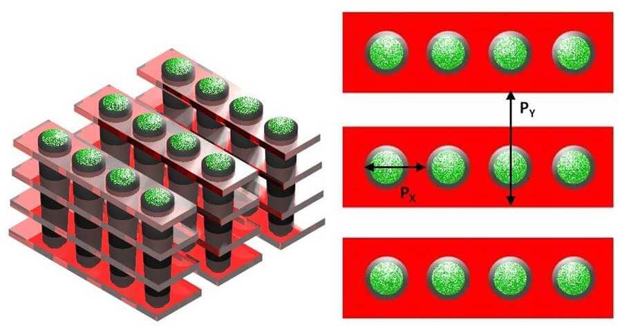
The problem is that these “litho-light” approaches have almost everything except the kitchen sink defining their cell pitches. This can be seen in the figure where the X and Y pitches are shown.
In the X pitch, there are three main parameters, namely: the diameter of the channel; two times the thickness of the memory dielectric; the hole-to-hole space. The diameter of the channel is defined by the ability to etch and fill the hole. The memory dielectric thickness is defined (it turns out) by electrical disturbs unique to a NAND string of cells; only the hole-to-hole space is possibly lithographically defined.
In the Y-pitch, there are four main parameters, namely: the diameter of the channel; two times the thickness of the memory dielectric; the gate conductor extension beyond the hole; the slit space. The gate conductor extension is defined by resistance considerations. The slit space is defined by the need to etch and fill the structure. In this case, etching has to be done both with wet etchants and dry.

In other words, all except one of the pitch-defining parameters are set by inputs that are extremely challenging to change.
The resulting inefficient cell sizes can only be compensated for by lengthening the strings. This however is also fraught with difficulty.
Let’s compare notes next December. ~ AJW