
At last week’s Memcon 2013, which took place Tuesday, August 6, 2013, at the Santa Clara Convention Center, Keynoter Bob Brennen, Senior VP at Samsung, talked about the need for New DRAM and Flash Memory architectures. Richard Goering summarized Brennan’s keynote very well in his blog post.
 Because Brennan’s responsibility is to manage Samsung’s System Architecture Labs, he talked about memory from a system-level perspective and mentioned my primary focus, their recently announced 20 nm 3D vertical NAND, only briefly. I read about this part in EETimes the day before. So I approached Brennan during the break and asked him how to get more information. He invited me to attend Samsung’s keynote at the Flash Summit, On Tuesday, August 13, in the same location. I am really glad I followed his advice and joined the very well attended event.
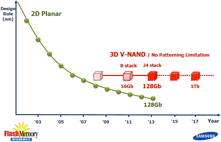
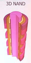
in a very humorous and memorable way, Jim Elliott, VP Memory Marketing in San Jose, and E.S. Jung, EVP/GM of Samsung’s Semiconductor R & D Center in Korea, presented the charge-trap concept and the architecture, features, and benefits of this 128 Gbits 3D V-NAND device; a non-volatile memory technology. The press release, issued on the same day, mentions many of the points Elliott and Jung made during their presentation and highlights the target application for the 3D V-NAND Flash: Solid State Disks (SSDs) for the enterprise market.
How might this 3D V-NAND impact through silicon via (TSV) interconnected, highly integrated 3D-ICs, like Hybrid Memory Cube (HMC) Wide I/O, High-Bandwidth Memory (HBM) and heterogeneous 3D-IC stacks?
After having my recent EETimes blog, “Semicon Shows support for 3D-ICs” labeled as “pollyannaish coverage”, I’ll attempt to provide more balanced comments about this remarkable achievement at Samsung.
Looking at the target application and functionality of this Flash memory, these non-volatile 3D V-NANDs clearly won’t replace volatile DRAMs comprising HMC, HBM and Wide I/O memories. Also, the integrated SERDES interfaces allow HMC and HBM to serve both as near and far memory, a feature Samsung’s current 3D V-NANDs don’t need nor offer.
Why is Samsung targeting the solid state drive (SSD) market with 3D V-NAND? Every time my old laptop told me “Vibration has been detected” and the disk stopped functioning, I dreamed of a MacBook Air with an SSD. Now I have one and really value SSD technology for its speed, low power dissipation, and of course absolute vibration resistance. Increasing SSD capacity while reducing power and cost per MByte, for mobile devices and especially for enterprise solutions, is clearly needed. The cost and technical benefits the new 3D V-NAND can offer for SSD applications will reward Samsung for developing it.
The fact that Samsung hinted: “These 3D V-NAND devices are not relying on smallest possible feature sizes, very expensive lithography and the related yield risks”, tells me that older, fully depreciated wafer fabs may be used to cost-effectively manufacture these devices. In addition, Samsung’s concept appears to be fully monolithic and avoids costly wafer thinning, handling and assembly processes. All manufacturing steps for the die are being performed in a Samsung wafer fab; simplifying logistics and the business model.
Samsung clearly states that its 3D V-NAND does not use TSVs to vertically interconnect the horizontal memory arrays. During wafer manufacturing, they etch trough up to 24 layers, but don’t give details how. Considering that the company’s new technology is covered by about 300 patents and is the result of a multi-year development effort, I can understand why they don’t volunteer this hard-earned know-how publicly.

If you are interested in the history and more technical details about 3D memories, check out the excellent 3D RRAM presentation Henry Chen, Ph.D. student with Professor Philip Wong at Stanford, gave. Like the slides of the Samsung 3D V-NAND presentation, both presentations can be downloaded here.
One more point about TSVs: They are integral building blocks of 3D-ICs. They not only enable very wide busses in 3D memory stacks, but also can interconnect individual memory die and stacks with logic chips or other functions, either directly or via an interposer. It remains to be seen if Samsung’s 3D V-NANDs can/will offer such arrays of TSV-like contacts for high bandwidth, short latency and low power connections with other die.
Bottom line: Samsung is positioning these 3D V-NANDs as building blocks for higher capacity, lower power, faster and lower cost SSDs, to capture a major part of this rapidly growing market with this impressive design. If, when and how they’ll modify the current 3D V-NAND to offer a non-volatile memory component as program store to complement HMC, HBM or Wide I/O remains to be seen.
By ramping up the 3D V-NANDs into production NOW, Samsung is demonstrating that utilizing the 3rd dimension in ICs is not only technically feasible but can also be done very cost-effectively. The competitive race for the best and most cost-effective 3D memory and 3D-ICs in general, has gained another, very promising contender.
How significant Samsung’s 3D V-NAND was a major discussion topic in yesterday’s Flash Summit Panel, moderated by Jim Handy. Micron’s Chuck Dennison, senior Director of NAND process integration, announced that Micron will also offer 3D NAND devices, utilizing their 16 nm 256 Gbit technology and their HMC experience as foundation for their 3D NAND product line. Again, see more about this panel in Richard Goering’s post. ~ Herb Reiter, eda2asic


Thank you. Great summary. This falls in line with other Flash providers with regard to 3D NAND. In reading SanDisk for example, the timing of deploying the 3D NAND has to do with cost as it relates to the change in the design. Not so much from a process design change (Within the existing tool set), rather from a design change that requires a significant investment in tooling. See attached.
http://www.theregister.co.uk/2013/07/23/sandisk_takes_the_bics_route_to_3d/
Really cool stuff though, and more for the “Queen of 3D” to track and follow
Readers,
As some supplemental reading about 3D NAND structured, in simple terms, i refer you to this article I read in Forbes’ Magazine. I’m not sure I agree with what is suggested in the title, With 3D Chips, Samsung Leaves Moore’s Law Behind, but contributor, Michael Kanellos, does a great job explaining the 3D architecture of 3D NAND as transistor stacking, which should not be confused with 3D ICs that are stacked die. http://www.forbes.com/sites/michaelkanellos/2013/08/14/with-3d-chips-samsung-leaves-moores-law-behind/
Interesting Forbes piece by Michael Kanellos – I know his work from having followed his writing at Greentech Media, where Michael reported on Solar and other forms of green energy. I’m intrigued by two things about Samsung V-NAND flash memory.
The first item of interest to me is to understand exactly how the stacked memory cells are addressed – is each stacked layer / cell independently addressable, or, are the cells somehow ganged together with their up and down neighbors?
The second item of interest to me in Kanellos’ piece comes from this line: “…Samsung has plenty of work ahead of it. It has to master mass manufacturing chips with these exotic channels. Managing heat and mechanical wear will also be problems.”
More color on that please Mike. We hear lots about managing heat in true TSV/3DIC stacks – are there similar concerns here in V-NAND?
Hello Rick, Thanks for the pointer to “theregister” above. Yes, SanDisk and Toshiba are also active in this space. I would be surprised if Hynix would not have a similar effort ongoing.
In addition to all the NONvolative technologies in development, we need an equivalent VOLATILE solution, to overcome the painful memory wall.
Do you know of any such efforts going on? If yes, where?
Herb,
Good afternoon and thank you.
You are correct with regard to SK Hyinx and 3D Nand. See below from earlier this year.
http://www.eetimes.com/document.asp?doc_id=1280909
As an example I can provide for a 3D solution in the Volatile Memory space, I would refer you to Tezzaron Semiconductor and the work they are focused on in the DRAM/Vol Memory space/applications.
http://www.tezzaron.com/about/about.html
http://www.tezzaron.com/about/Press/Releases/1212_Ziptronix.html
Hope this helps.
Have a great day
There are alternatives to TSVs as fundamental building blocks to 3D IC intergration. As I presented last year at RTI 3D, the Ziptronix DBI(r) technology provides high density, scalable, interconnect which can be implemented during stacking at wafer scale. Stacking at wafer scale provides lower cost and higher yields then die level stacking when designers implement strategies for self test and repair. Today Ziptronix is involved with top tier memory suppliers for advanced 3D memory solutions at wafer scale.