

As its name implies, the International Wafer Level Packaging Conference (IWLPC) initially covered wafer-level packaging (WLP) technologies. As all conferences do, it soon expanded its scope to cover basically all advanced packaging topics including WLP, fan-out wafer-level packaging (FOWLP), 2.5D/3D, and advanced manufacturing and test, etc. Statistics from this year’s show include:
- 809 Attendees
- 75 Exhibitors
- 19 Countries Represented
- 45 Technical Papers
Let’s take a look at a few of the key presentations at IWLPC 2018.
WiSpry / Amkor Europe
Rameen Hadizadeh and his co-workers at WiSpry and Amkor Europe discussed “Wafer-Level Fan-Out for High-Performance, Low-Cost Packaging of Monolithic RF MEMS/CMOS”. They started out with an astute comment that we all should pay attention to: “Packaging, in general, is detrimental to RF performance, regardless of device technology.” Their listing of packaging challenges included:
- Thermal overstress – polymer cure, solder reflow
- Mechanical overstress – residual film stress, EMC underfill pressure, wafer back-grinding
- Triboelectric charging – wafer dicing, tape/de-tape, pick and place, package handling
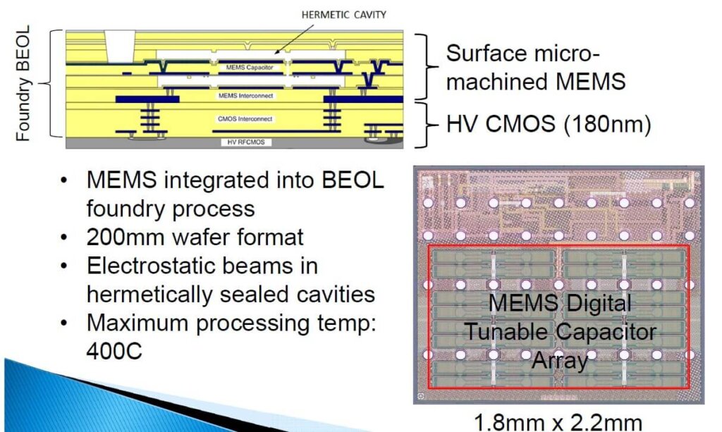
The hetero- Integrated device that they were attempting to package was a MEMS device being driven by CMOS circuitry as shown in Figure 1.
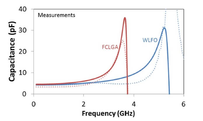
They compared a flip chip land grid array packaging solution to a FOWLP solution and found that the FOWLP solution could be manufactured with a 56% package height reduction at a 48% cost savings. In addition, the FOWLP packaging allowed usage out to a higher frequency (Figure 2).
Veeco / Brewer Science
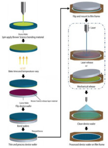
Kenji Nulman, in a joint presentation between Veeco Instruments and Brewer Science, discussed temporary bonding and the challenges posed by post debond cleaning. Temporary bond /debond (TB/DB) of wafers has been widely applied over the last decade in WLP technologies, such as package-on-package (PoP), FOWLP, and 2.5-D and 3-D integration using through-silicon via (TSV). This normally follows a process flow as shown in figure 3, where the final step requires removal of any residual bonding material from the thinned device wafer supported on a film frame.
In this case this was optimizing a process removing BrewerBOND® 305 Bonding Material using d-limonene, generally viewed in the chemical industry as a natural “green solution” to previous degreaser materials like chlorinated hydrocarbons. By optimizing time, temperature and spray pressure they were able to achieve wafer-to-wafer consistency at high throughput.
Xperi – D2W Hybrid Bonding
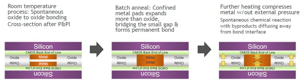
Guillian Gao of Xperi discussed the company’s attempts to develop a hybrid bond interconnect technology suitable for die-to-wafer (D2W) bonding. Since Ziptronix originally developed what has been come to be known as direct bonding or hybrid bonding, the technology has only been commercialized for wafer-to-wafer (W2W) applications. Since their acquisition by Xperi, they have been working to develop a D2W process which could allow them to access the stacked memory market.
As a refresher, the DBI process flow is shown in the diagram below.
For today’s thermocompression bonding (TCB) solutions the μbump and underfill act as a buffer layer and basically encompass the contaminants, whereas for hybrid bonding the bonding surfaces must be pristine. Contaminants reportedly can come from:

- Dicing
- Particles from the dicing process
- Organic contamination from the dicing tape
- Metal corrosion
- Die handling
- Organic and inorganic contamination can happen in every step of the process: die transit process between prep steps, inspection, pick, place, ……
In addition, there is a problem with chemical mechanical planarization, because for D2W bonding, large bond pads are required to enable large misalignment tolerance (4-7μm) and these large pads result in more Cu dishing. They require shallow and uniform Cu recess of large pads (5 to 15μm diameter) across the entire wafer.
Xperi claims to have developed a process to control these issues for 200 and 300mm wafers although we are given little info on what makes the optimized process flow work.
They now claim that bonding pitches of 40μm, 20μm, and 10μm have been demonstrated and a volume production ready process has been developed
- All die preparation on the dicing tape
- Direct P&P from dicing tape for bonding
- Stacking of up to 20 layers has been demonstrated
Samsung FO-PLP found in Samsung Galaxy Watch
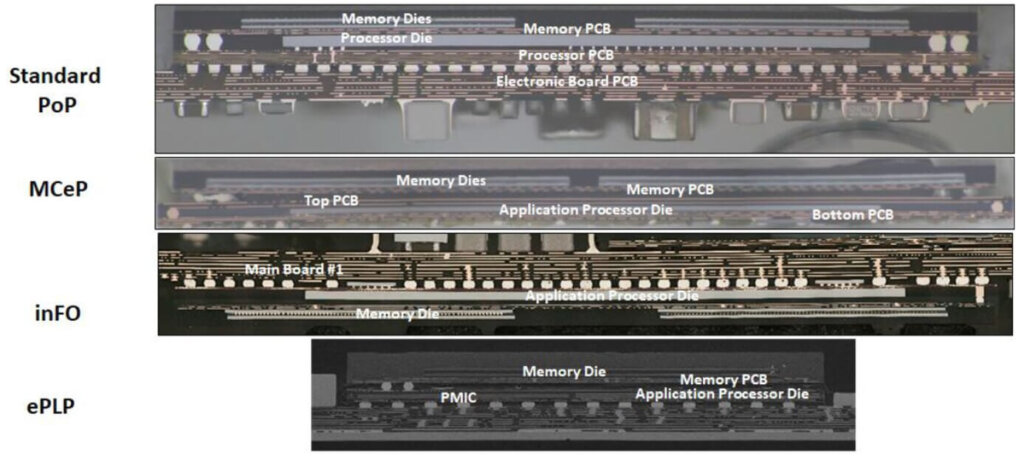
Samsung’s new fan-out panel level process (FO-PLP) was discussed recently in IFTLE 389, “Samsung 2μm L/S Panel Level Packaging Technology Revealed at ECTC.” System Plus consulting has now revealed finding Samsung Exynos 9110 with ePLP. In the first generation of Samsung’s FO-PLP, Samsung has managed to bring together an application processor engine (APE) and a power management integrated circuit (PMIC) in the same package in a system-in-package (SiP)-PoP configuration.
This solution is integrated on the main board of the Samsung Galaxy Watch. The module includes the Exynos 9110 application processor and Samsung’s Power management system in a single package < 80 mm². This is only the second multi-chip fan-out device they have found on the market.
In an interesting slide (Figure 5), SystemPlus compares cross sections of the standard PoP to Shinko’s MCeP to TSMC’s InFO to Samsung’s ePLP.
For all the latest in Advanced Packaging stay linked to IFTLE……………


