


…For while the tired waves, vainly breaking,
Seem here no painful inch to gain,
Far back, through creeks and inlets making,
Comes silent, flooding in, the main….
(Excerpt from Say not the Struggle Naught Availeth, by Arthur Hugh Clough. 1819–1861)
Sitaram Arkalgud, Invensas, quoted this verse to me yesterday over coffee, as we sat discussing the 3D panel he had just moderated as IWLPC 2013 wrapped up its 10th year. It expresses perfectly how it appears the high volume manufacturing (HVM) ramp of 3D ICs will take place. I’ve attended more than my share of keynotes, plenary talks, and 3D focused panels where experts from across the supply chain discuss the readiness of 3D ICs for volume manufacturing. For some time, we’ve heard the same laundry list of challenges that need to be solved before we go to HVM– thermal, test, design tools, thin wafer handling, infrastructure, reliability, cost reduction – but what is becoming clear (at least based on this year’s 3D Thursday plenary talk and 3D panel at IWLPC 2013) is that this list needs to be revamped. Most anyone will tell you that aside from the thermal issues, technologically we’re ready (if we weren’t, would Xilinx be manufacturing products?), that the infrastructure is in place (TSMC, GF, ASE, Amkor all claim to have 300mm 3D TSV lines), and that we can iron out the ‘who-does-what issues”.
This brings us to a revised laundry list with one item on it: cost reduction. As Rajiv Roy of Rudolph Technologies explained, customers are still trying to figure out other ways to get the performance they need based primarily on cost structure. If the device is 90% of the desire performance, they will go with the cheaper alternative. But this Band-Aid approach can only last so long. And guess what? If you’re waiting for through silicon vias (TSVs) to ever cost the same as wire bond products, you’ll be waiting a really long time. As Arkulgud said to me, “we’re not building TSVs to replace wire bonds.” What TSVs really replace is the need to shrink to smaller nodes – and in comparison to that, TSVs offer a cost benefit.
In his plenary talk, This Changes Everything, Invensas’ Simon McElrea drove that point home. McElrea talked about “personal power”, and how we now carry more access to data in our pockets than was needed to put a man on the moon. He also showed how our behaviors and habits have changed due to the smartphone and other mobile devices, such as using our phones to check the time rather than relying on a wristwatch, the way we consume media, and the way we shop. Ultimately, in what McElrea called a “knowledge economy” driven by the Internet of Things (IoT,) we need solutions that give us greater access to data at higher speeds, with lower power consumption, better performance, and increased bandwidth.
McElrea talked about strategic “inflection points” and that 3D IC is the one of these, because its becoming increasingly expensive to produce the next node of technology. Stacking CMOS using TSVs gives us multiple orders of magnitude of power savings, whether you’re talking about mobile battery life or data centers. “3D is ubiquitous. It’s not just a memory solution, it’s a key building block,” explained McElrea. “The OSAT roadmap doesn’t look anything like what it dis 3-5 year ago. It’s a whole different world. We call it Interconnectology.”
During the IWLPC 2013 panel, 3D HVM, Are We There Yet panelist Jim Walker of Gartner, also talked about interconnectology going vertical in 3D and TSV, and how this is driving the future. Ultimately, he said we really have to go 3D on either the chip or the package. And while we’re waiting to see who’s going to jump on the bandwagon first, he offered this paradigm to consider: technology leaders in one wave rarely survive to become the technology leaders of the next (think Wang, Kodak, Digital, and Compaq). Additionally, the leaders who define each wave frequently did not exist in any significant way in the previous wave (think Amazon, Google, Facebook.)
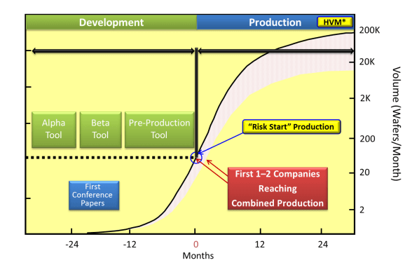
Getting back to the big HVM picture, before we can determine how close we are, we have to understand what HVM means. Arkalgud shared this ITRS Technology Production “Ramp” Curve to demonstrate where 3D IC falls on the spectrum. Based on these parameters, Arkalgud says that with Xilinx’s entire Virtex product family going to 3D, Tezzaron in low volume production of stackable 3D memory, and Micron shipping engineering samples of the Hybrid Memory Cube (HMC), we’ve surpassed the inflection point where development gives way to production. We’re ready to knock down all the barriers and “go all green”, (referring to Xilinx’ Suresh Ramalingam’s slides in his panel presentation.)
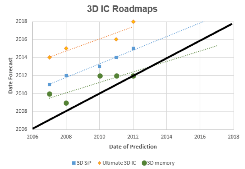
Laura Rothman Mauer, SSEC, talked about how the 3D IC roadmap continues to be pushed out, and by analyzing the various market research roadmaps, she devised her own roadmap by plotting prediction dates in the year they were predicted, and connecting the points to create a trajectory across the real timeline. As you can see, 3D Memory hits the real time line early 2013, which is close to the target if you consider the HMC. 3D SiP and the ultimate 3D IC are at least not on parallel trajectories with the real timeline, but if this is accurate, we won’t be seeing them cross the line any time soon.

After listening to all the reasons why 3D IC production keeps being pushed out for so long, here is my take: when 3D IC reaches HVM has less to do with the manufacturablity of the devices at volume, and more to do with the customers deciding its worth the investment. It’s not that the device can’t be built, its that it can’t be built the cost the customer is willing to pay. When will they willing to pay for it? “When there’s no other way to do it,” predicted Mauer. And if the readiness slides Suresh Ramalingam, Xilinx and Abe Yee, nVidia showed during the panel are anything to go by, that time differs from company to company.
While Xilinx shows the green light in readiness across the board, nVidia is still showing red areas. Mostly, they are waiting for the price to come down. Yee did admit that the company is “willing to pay a little more, but not a lot more” for 3D devices than they do for conventional wire bond or flip chip packages. He also admitted that the next-generation GPU will be a 2.5D interposer, but didn’t say when that would happen. “We’ve been driving Moore’s Law for 10 years, but even if Moore’s Law continues, we’re hitting a bottleneck at the system level because of bandwidth limitations with talking to the memory.” he explained. “We need all the data we can get to crunch information to keep it from stalling… we have to go to a 3D solution on graphics chips, and memory…we need lost of DRAM close by, which calls for real 3D solutions (4-8 stack memory.)”
So its been established: this industry clearly NEEDS 3D to go forward. But it will not come in as a flood but as a trickle that will grow to a steady stream, finally silently flooding the main. ~ F.v.T.











Francoise thx for sharing with us the highlights of 10 th IWLPC.
Was there any discussion on the stress effects of Cu filled TSVs on CMOS device performance or effect of Keep Out Zones on routability and Bandwidth ?
For a comprehensive take on 3-d materials, process, design and performance you could look up 2 of my articles that CSR and SST published, both in Sep 2013.
Hope we would be able to think our way out of the 3-d Box Canyon that we seem to have walked into.
If I may jump in, Dev, the one mention of KOZ and bandwidth was in the context of discussing various interposer technologies. Si was deemed to have the optimal combination of minimizing KOZ and high bandwidth. If memory serves me correctly both Xilinx and nVidia mentioned it.
I wasn’t there, so can’t answer the question directly. But I would like to point out that the stress effects of copper-filled TSVs and chip-package interactions with thinned and stacked die has received an enormous amount of attention. While this is an important issue, I agree that the biggest issue is cost: we need to continue to drive down the cost of the wafer processing and assembly technologies, address the supply chain issues around known good die and assembly yield, and identify the “killer” applications where the functionality, performance, and form-factor improvements justify the development and manufacturing costs. There are some remaining manufacturing issues, such as temporary bond and debond, thin wafer and die handling, scaling to higher aspect ratio TSVs and thinner wafers, low-cost thermo-compression bonding, etc…, and these are being addressed. Some other important and well-known issues include pathfinding, design, EDA tools, test, standards, thermal management, etc…. The relative importance of these, relative to stress management, will vary widely depending on the application and implementation.
Thank you Larry and Rajiv for your responses to Dev’s question. I’d like to add that there were not any papers that specifically addressed the issue of stress effects of Cu filled TSVs, nor was their discussion during the panel that I recall. There was one paper that discussed using polyimide films as dielectric layers reduce the stress and warpage of the interposer or die stack overall, but it was more in reference to the stress caused by thin wafer handling and did not mention stress caused by Cu TSVs or KOZ. I did have a chance to chat with Paul Lindner, of EV Group, about the company’s nanofill process using polymer to fill Cu lined TSVs to reduce stress, but this is more for coarse TSV applications like BSI CIS technologies. More on that to come.
How does the question of a stress related KOZ arise for Interposers ? Neither of these 2 have any active devices in their interposers, be it Si or glass, just interconnects. TSV induced radial stress or gross warpage of the substrate / interposer would probably have not that big an effect on the dielectric thickness / interconnect parasitics / bandwidth, right ? Or am I missing something here ?
( cont’d ) such as second order localized CPI effect of the TSVs in the Interposer on the functional chips FC bonded over them ?
Won’t the Cu RDLs (and proportionate to the metallization) especially when on one side of the interposer induce stress?
Hi Rajiv sure they ( RDL ) would but my original question was about stress effects from the differential expansion of Cu in TSVs on the switching of transistors and what it does to the variation of rise times based on where the transistors are located w.r. to the TSVs on an active chip itself ( the secondary CPI stresses from TSVs or RDLs in Interposers under the chip are not that important ). This is a major design issue that received a lot of attention, as far as modeling goes, several years ago but since most of the experimental work was being done at non IDM co.s there has not been all that much characterization work. IMEC has picked up on it only recently. But Tezzaron has been the most intelligent about it. They have just gotten rid of Cu and replaced it with W. They have done several other equally smart things about their process which totally sidesteps the problems plaguing the mainstream approach to TSVs. For more details you can read my articles in SST and CSR of Sep 2013. But looks like this showstopper topic was not covered at IWLPC. Talking about cost is premature & simple minded when one is stuck in a technology blind alley.
Dev – Thanks for the kind words and your astute observations.
As Dr. Gupta so rightly states, tungsten is the best for TSVs! But Tezzaron does sometimes use copper. Tungsten is deposited, not plated, so it can be problematic for TSVs deeper than 20 microns (too much overburden). Fortunately, 20 microns is more than enough for our wafer-to-wafer stacking and for most of our die-to-wafer projects. However, in 2.5D interposers, and in dies that must be tested before bonding, we need deeper TSVs. In those cases we use copper – very carefully – and we impose the necessary design restrictions to cope with the thermal mismatch.