
The 10th International Wafer-level Packaging Conference (IWLPC 2013) was held at the DoubleTree Hotel in San Jose this week. I had an opportunity to attend part of the technical sessions and the keynote Invensas’ president, Simon Mc Elrea, presented on Thursday morning. I also enjoyed the 3D Panel, moderated by Sitaram Arkalgud, formerly at SEMATECH, now at Invensas, on Thursday afternoon.
If you know that I strongly believe in a very bright future for 2.5/3D ICs, you won’t be surprised about my 3D focus and positive attitude in this article. If you don’t know me, please read my comments below with an open mind.
First a few words about the general sessions on Wednesday and Thursday:
Compared to previous years, interposer-based, so-called “2.5D ICs” were at least mentioned, if not discussed in-depth, in most of the sessions I attended. I clearly noticed that packaging experts are flexible and creative and have mostly integrated 2.5D-specific development efforts into their general development programs. Higher power-density, tighter pad-pitches, power- and signal integrity, warpage and other challenges are common to “2D SoCs” and 2.5D designs, so it makes a lot of sense that packaging experts have made 2.5D technology part of their mainstream development programs and resource it accordingly. It’s a different story for 3D IC (vertically stacked die in a package), but more about that later.
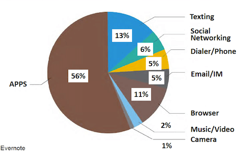
For me the highlight of this year’s conference was McElrea’s keynote on Thursday morning. The title “A Consumer Driven Market – This Changes Everything” triggered my hopes for a thought-provoking message. McElrea far exceeded my expectations. He substantiated his message with a series of facts about changing consumer behavior, for example: only 5% of smartphone usage by consumers is as a phone, and 95% is for other purposes! McElrea also clearly explained why continued scaling of silicon (feature sizes) is going to give way to “package scaling”.
Simon closed by highlighting that Invensas anticipated this radical transition to lower power, smaller, faster and more intelligent mobile internet devices. They have been investing in what Invensas calls “Interconnectology” for many years already, therefor are well positioned to serve today’s market needs in support of the new consumer requirements, also for 2.5 and 3D-IC packaging technology.
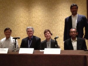
The afternoon panel, titled “3D High Volume Manufacturing – Are We There Yet?” complemented Simon’s keynote very well. Sitaram Arkalgud, also from Invensas, was the moderator, Laura Rothman Mauer from Solid State Equipment Corp (SSEC), Suresh Ramalingam from Xilinx, Jim Walker from Gartner Technology and Abe Yee from Nvidia the panelists.
While Walker’s message did not directly answered the question of whether we’re there yet, he did provide some compelling insight as to why 3D is needed. He focused on the Internet of Things (IoT) as a key driver for 3D and TSVs. Mauer reported from an equipment supplier’s perspective, noting that IDMs and OSATS are at various stages of development. Some are in low-volume production with development work going on. Everyone is looking for lower cost and higher yield processes, and are therefore interested in testing alternative methods such as wet etch for TSV reveal, thick film strip, single wafer wet etch for finer pitch UBM and RDL, and flux-related processes. She noted that IDMs have internal product plans and schedules that will determine HVM timing, and pointed to Micron, Xilinx and Tezzaron as examples. She said the OSATS need to be ready to support their customers, and all the top tier OSATS have announced readiness.
From the customer perspective on readiness, Ramalingam conveyed a clear YES, because Xilinx is in production with multiple FPGA die and/or SERDES die on an interposer and works hard to expand this winning product family. Alternatively, Yee expressed a clear NOT YET, primarily because Nvidia needs lower components cost to successfully combine memory with their GPUs on interposers. Yee went a step further and projected that Nvidia’s graphics roadmap requires 3D IC technology as the following step to meet future market requirements.

As mentioned above, IWLPC demonstrated clearly that 2.5D interposer-based designs, are possible today. For less cost-sensitive systems the space and power savings, together with significant increases in bandwidth and overall performance outweigh the currently higher component cost, versus traditional technologies.
The general sessions and this panel confirmed that vertically stacked die interconnected with TSVs are still several years away from production volumes. EDA tools for high-yielding logic partitioning, verifying and testing of these complex 3D ICs are still missing. Higher-throughput manufacturing equipment is needed to bring cost down. Business models for heterogeneous integration and multi-company cooperation still need to be agreed upon.
As I outlined in 3D InCites several weeks ago, Samsung already introduced their 3D vNAND. The other major memory vendors are developing monolithic 3D configurations, by stacking multiple (even many) memory arrays vertically, interconnecting them with very high aspect ratio vias. These monolithic stacking concepts will start production in 2014 and these lower cost memory stacks will accelerate the market momentum towards broad deployment of 2.5/3D-ICs. ~ Herb Reiter, eda2asic


Bottom line is we need a demand of ~200,000 WPM to drive cost down. Less is only feeding specialty applications where cost is second to drive performance and needed to support value added systems.
The technical barriers such as testing and sorting KGD to lowering costs are especially true to low volume. With high volume these issues get the funding needed to be resolved.