


An industry colleague commented to me recently that the press seems to have lost interest in 3DIC. As probably the industry’s most avid follower and writer of 3D related news, I had to disagree – its not that we’ve lost interest, its just that there seems to be a lull in new information. Either that or there’s lots happening behind the scenes that can’t (or won’t) be revealed. To prove my point, I spent some time looking around for new stories, and came up with a solid technical feature, a roundtable discussion and a solid editorial addressing 2.5D and 3D ICs, all of which appeared in the past week.
On the technology development side, I see activity in metrology and inspection processes for 2.5D and 3D ICs, work being done to fine-tune 3D TSVs into smaller semiconductor technology nodes, and on the other end of the spectrum, what 2.5D and 3D packaging will do to the PCB market. (Once again I’m struck by how 3D adoption will affect the entire microelectronics supply chain.) Let’s take a closer look at these stories:
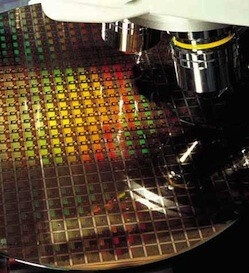
There are a host of metrology and inspection needs for 2.5D and 3D ICs, which is why it’s becoming more of a hot topic. In a roundtable discussion on metrology and inspection, conducted by Mark LePedus and posted recently on SemiMD, Robert Newcomb, of QCept Technologies, explained that there is a whole new class of concerns such as sub-monolayer metallic contamination within the device area. “If these wafers need to be thin, and I need to expose the TSVs, I start seeing copper defectivity and sub-monolayer issues.” He explained, “Now, I am trying to stack multiple known-good die. As we package these known-good die in 3D structures, and if you have one mistake like sub-monolayer copper residue, that will make multiple known-good die no longer any good.” Kevin Heidrich, vice president of marketing and business development at Nanometrics added that because the known-good wafer needs to be integrated, it ends up requiring double metrology and double inspection. On top of that is the added complexity due to the TSVs. “Metrology and inspection for that whole flow must be addressed for cost, performance and reliability,” he noted. Offering his two cents, John Allgair, senior member of the technical staff at GlobalFoundries, said “If I look at the 3D TSV side, the idea of stacking structures has created a need for new tools. We have been looking at new techniques, which should work out reasonably well. We are making pretty good progress.”
Acoustic micro-imaging is one inspection technology that’s seeing lots of activity, particularly with 2.5D interposer inspection, according to an article titled First 2.5D Acoustic Imaging authored by technology journalist, Tom Adams, recently published in ElectroIQ on behalf of Sonoscan. Adams writes about how AMI provides a non-destructive way to inspect wafer bonds in 2.5D interposers. Apparently AMI is becoming very popular during development partly because of the variety of 2.5D devices needing evaluation. According to the article, AMI achieves what X-ray alone cannot: revealing the integrity and bonding of microbumps to solder bumps, in addition to inspecting underfill layers for voiding. The article offers a comprehensive overview of how AMI detects these defects. (Incidentally, the author included a disclaimer regarding the confidentiality of the 2.5D samples being evaluated as a reason why there are no AMI images. This points to the stealth mode I’m talking about.)
Speaking of stealth mode, according to a recent post by ElectroIQ’s Phil Garrou, GlobalFoundries is reportedly “taping out a 3D design with an undisclosed customer” and is working on 2.5D with two others.” It also appears that while GF initially intended to ship 2.5D and 3D chip stacks in 28nm and 20nm technology, they’ve abandoned 28nm in favor of 20nm and pushed volume production from 2014 to 2015.

And lastly, offering a novel perspective on the future of 3D IC technology, I read a great post by All Programmable Planet’s Brian Bailey, who predicts that 3D IC will ultimately be a replacement for printed circuit boards (PCB). He says PCBs will become “nothing more than a holder with the ability to add connectors and perhaps a few components that cannot be economically integrated within the chip package”. In supporting this prediction, Bailey points out that in 2.5D technology, the silicon interposer acts like a PCB, and that a more efficient use of that silicon is to make it active as well, although its admittedly more difficult to put TSVs in active silicon than passive. Technical hurdles aside (Bailey does enumerate on this) he writes “Altera will eventually go with 3D technology; Intel will have to go in that direction; and, in fact, the entire industry will have to embrace 3D technology — any issues will be resolved such that it becomes economic and indeed essential for maintaining high yield.” Personally, I like Brian’s upbeat attitude; the whole post is worth a read.
As you can see, 2.5D and 3D IC are still newsworthy topics in the semiconductor space. We may have hit a slight dry spell – but I expect things to pick back up as ECTC 2013 approaches, followed but SEMICON West. Such major industry events always draw the trade press and inspire bursts of inspiration.


