
Since the early days of 3D InCites, as a member of our technical advisory board, Sitaram Arkulgud has been one of my go-to guys when I had a question about various 3D processes and technologies. There are few people in this industry that have been as enthusiastically optimistic as I am that 3D ICs will be commercialized; and Arkalgud actually knows what he’s talking about.
As director of Interconnect at SEMATECH, Arkalgud lead the 3D interconnect program with the goal of taking 3D IC processes from feasibility to high volume manufacturing (HVM). He recently left that position to take one as VP of 3D technologies at Invensas Corp., an interconnectology solutions provider for advanced mobile applications, where he will now get to foster 3D ICs the rest of the way to commericialization. I recently spoke with Arkalgud about this opportunity and his decision to make this career transition from R&D to manufacturing.
While Arkalgud first began his semiconductor career in the manufacturing environment, having put in time at both Infineon/Quimonda and Motorola, he really found his niche in the R&D consortium environment at SEMATECH. “When I first heard about 3D technology in 2004, it seemed really cool but nobody wanted to take the risk.” he explained. “SEMATECH is a great place to be when you have something teetering on the edge. You can take that risky technology, incubate it, sharing the risk and cost of development.” And that’s what he did as director of SEMATECH’s 3D interconnect consortium, nurturing 2.5D and 3D to the point that it is now in the early phases of market adoption.
“Once it started taking off, I had this feeling that things were happening and we were on the sidelines,” he explained. Focus shifted in the program to scalability, preparing for the next technology node and determining transition points; all the elements of technology maturity. In the meantime, “people on the outside were actually making parts,” said Arkalgud. “3D is personally exciting for me and I just want to see parts made using it.”
When the opportunity came to join Invensas and be part of the action, he took it. As a wholly-owned subsidiary of Tessera, the IP start-up launched two product lines last year – xfD and BVA – that leverage the existing infrastructure to provide high-density “bridge” solutions to meet performance and power requirements of next-generation mobile and memory devices. But 3D ICs are next on Invensas’ roadmap, and they’ve brought in a ringer to help make it happen.
“It seemed to be the right place to go,” said Arkalgud. “Invensas is a small group, but very nimble, with lots of funding behind it. It’s a very exciting place to be.” He also said there would be more constraints to deal with at a larger company, and in terms of manufacturing, it would be a good transition from SEMATECH.
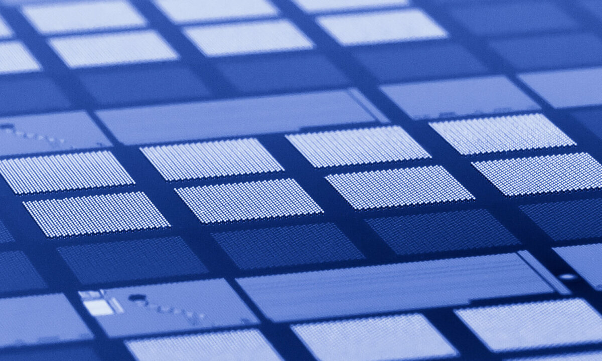
Next month at the IMAPS Device Packaging Conference in Scottsdale, AZ, Arkalgud will deliver a keynote address titled “2.5 and 3D – Scaling Walls”, where he will talk about how economics are driving the industry, and that the main reasons for scaling 3D is to reduce cost. “There’s lots of optimization that needs to happen, such as improved yield and scaling the TSVs themselves. Shorter, narrower holes require less material, although the pain of handling thinner die will be handed on to assembly,” he explained. “In the CMOS world, it takes 3-5 years to develop the next technology. The time to worry about this is now. If the next nodes are coming in 2013/2014, we need to think about what comes next.”

“3D is the logical next step,” says Arkalgud. “It brings everything to the table in terms of power and performance. However, it still needs a little more maturity before it reaches HVM, such as a lower price point and supply chain maturity.”
Just as he helped 3D get its start at SEMATECH, Arkalgud is looking forward going the distance and seeing it through at Invensas. ~ F.v.T.


