
With heterogeneous integration, 3D, and advanced wafer-level packaging technologies officially declared the rising stars of the semiconductor industry, materials, process and equipment suppliers have pulled out their shiniest bells and whistles. Here’s a sampling of news and products that were on display at IWLCP 2018, October 23-25, 2018 at the Doubletree Hotel in San Jose.
Indium Corporation’s 3D Coming Out Party
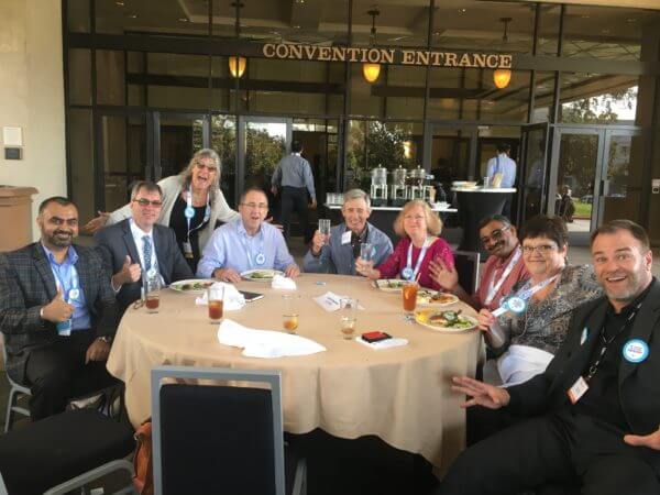
Many will tell you that when it comes to 3D technologies, it’s all about the materials. So, I asked Dr. Andy Mackie, Senior Product Manager of Semiconductor and Advanced Assembly Materials at Indium Corporation, when the company was going to jump in the 3D ring. Turns out, they’ve been in stealth mode for some time. IWLPC 2018 was their official coming out party for their flux products targeting 3D memory stacks. I guessed high bandwidth memory (HBM); Mackie couldn’t say (Figure 1).
Bump fusion fluxes are being used after standard through silicon via (TSV) plating and Cu pillar/micro-bumping processes. Stripping photoresist post-bumping leaves the bumps overburdened with organic and oxide residues that reduce solderability and planarity of the surface. These fluxes are spun on and then reflowed, removing oxides more effectively than gas-based processes.
Another important flux development for Indium Corporation, says Mackie, is its ultra-low residue, which is compatible with all types of underfill and can be used in mass reflow. The ultra-low residue also supports thermocompression bonding (TCB), versus switching to the disruptive non-conductive film (NCF) approach.
While NCF works if you are stacking 8-12 memory die, says Mackie, there are issues with implementation beyond that. Indium Corporation’s answer is a dipping process using ultralow residue (ULR) flux, followed by capillary underfill. When you’re integrating a memory stack on a controller, it’s important to have extremely low residue, explained Mackie.
NXQ Inc. Takes Mask Aligners to the Next Level
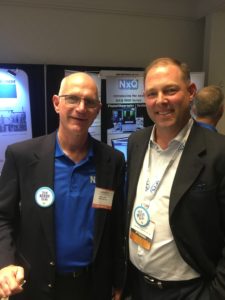
I caught up with Keith Cooper, Neutronix Quintel (NXQinc.com), and learned about the company’s latest mask aligner offering, the NXQ 9000 (Figure 2). Cooper says this is the world’s first web-based large format proximity stepper and can handle substrate sizes measuring 300mm x 300mm or larger.
Targeting flexible electronics and wearable devices, the stepper features unique roll-to-roll processing to create thin film metal masks on polymer mesh substrates. Cooper says the most exciting application for this tool is in manufacturing near field communication (NFC) sensors used to protect consumers from counterfeit versions of alcohol, medication, or make-up.
This latest addition to NXQ’s mask aligner family joins its legacy manual tool, the NXQ 4006, a university lab workhorse; and the NXQ 8000, a modular production tool for backside alignment processes that can be either manually loaded or be integrated with a robot in the field.
New milestones for Xperi’s DBI™
Partnering with UMC
Xperi’s big news, according to Abul Nuruzzaman, senior director, product marketing and new business development, is its partnership agreement with UMC, the world’s third largest foundry, for its Direct Bond Interconnect (DBI™) technology.
With Xperi as the technology provider and UMC as the manufacturer, this proprietary low-temperature, hybrid bond interconnect technology will now be available in volume production for a broader application space, including image sensors, RF, MEMS, analog mixed signal, touch displays, systems-on-chip (SoCs) and more.
The partnership arrangement gives UMC customers several options for implementing DBI into their products, explained Nuruzzaman. Xperi’s new 3D Lab is fully outfitted for customer development and demos. UMC’s license covers low volume production on behalf of its customers. Once the customer reaches higher volumes, they will need to license DBI directly from Xperi.
DBI for die-to-wafer
Proper wafer surface preparation is critical to successful DBI. While these challenges have been addressed in wafer-to-wafer) W2W DBI, which is now in high volume production, there were some remaining issues for die-to-wafer and die-to-die implementation of the technology.
As part of IWLPC’s technical program, Guilian Gao, Xperi, showcased the company’s recent success in implementing DBI in die-to-wafer and die-to-die stacking processes by addressing two critical challenges:
- Controlling dishing through unique CMP processes that result in shallow, uniform, and well-controlled Cu recess on 5µm (or greater) bond pads.
- Minimizing particles caused by dicing on the die surface prior to bonding by using a protective coating and cleaning process.
According to Gao, both challenges have been successfully addressed. 20-die stacks on 300 mm wafers have been demonstrated (Figure 3)
Revolutionizing Thin Wafer Handling
Temporary bonding and debonding (TB/DB) for thin wafer handling has long been a challenge for a number of semiconductor technologies, including 3D integration with TSVs, MEMS manufacturing, and compound semiconductor manufacturing processes.
Conventional TB/DB approaches require intermediary layers, adhesives, and clean steps, and often are plagued by low yields caused by damage to fragile substrates during the debonding step.

To address this, start-up Eshylon has developed a mobile electrostatic carrier (MESC) platform that addresses many of the process challenges associated with conventional TB/DB approaches, according to Chip Maschal, VP global sales, Eshylon. For example, plasma dicing can be performed without worrying about adhesive residues. High-temperature applications can be supported without concern for CTE mismatch. Most recently, the addition of a Y2O3 coated mobile carrier supports dry etch processes.
Seeing is believing: see the MESC in action here:
We are watching @eshylon electrostatic temporary bond and debond. This could solve thin wafer handling issues for multiple applications like #compound-semi #3DIC, #MEMS and more. pic.twitter.com/Oi2zYxnJHd
— 3D InCites (@3DInCites) October 24, 2018
Debonder For Fan-out Wafer Level Packaging
Known for its thermal chucks used to for wafer reliability testing, 50-year-old ERS is now in the debonding business, says Klemens Reitinger, CEO. They’ve been providing Infineon with solutions to test devices at temperature – hot or cold – for years.
Because of the company’s expertise in thermal, Reitinger said they were asked to develop a debonding tool that would use thermal treatment to address warpage in embedded wafer level ball grid array (eWLB) fan-out wafer level packaging (FOWLP).
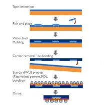
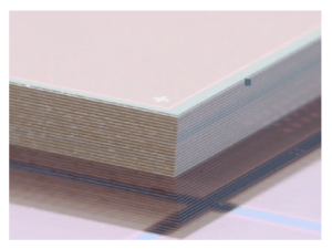
In chip-first (RD-last) FOWLP, plastic or metal carrier wafers are laminated with double-sided, sticky tape. Known-good dies are picked-and-placed followed by overmolding. The reconstituted wafer is then debonded from the carrier using a thermal release process, followed by RDL (Figure 4).
One of the challenges with this process is the occurrence of die-shift during the debonding step, as well as wafer-warpage due to the coefficient of thermal expansion (CTE) mismatch between the molding compound and the Si die.
According to Reitinger, the ERS ADM3300 fully automated debonder and warpage adjuster features a proprietary thermal process which is applied after debonding, to reduce and control the warpage of the reconstituted wafer. Specially designed temperature chucks enable uniform application of temperature into the package. This also allows for more predictable die shift, so it can be dealt with, said Reitinger.
This tool is designed to support 300/330mm wafers, but a new tool for panels is in development that will both 600×600 and 700×500 panel sizes.
“We have to be flexible, the machine is expensive and complicated, standardization would be nice, but we are years away from standardization,” said Reitinger.
See our tweetable moments from #IWLPC2018 here. That’s a wrap, from IWLPC. ~ FvT


