
Last week (November 6) STATS ChipPAC issued a press release announcing that its advanced eWLB provides a platform for 2.5D and 3D technologies. In search of further information about this, I found a feature article recently published in Solid State Technology that explained how eWLB can be leveraged for 2.5D and 3D packages. I still had a few questions how it all works, and had the opportunity to get those answered by Tom Strothmann, of STATS ChipPAC, at IWLPC (Nov 7,8 in San Jose).
eWLB as a 2D/2.5D Solution
I was confused about how eWLB could be used as an interposer, but Strothmann explained that it’s really about using eWLB in place of the interposer, essentially achieving 2.5D functionality by embedding heterogenous chips (logic) and (analog) in the mold compound, and then putting a redistribution layer (RDL) on top of that (either one or two layers).
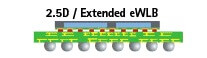
He said with fan-out processes, they are able to achieve a 10µm line space and two layers of RDL. Strothmann explained that the main purpose of an interposer is to enable pitch translation between the package and the board. “eWLB achieves that by doing routing and fan-out as part of the RDL layers.” he explained. An added bonus is an overall thinner package at a lower cost because of the elimination of the interposer. So this isn’t actually a 2.5D solution. What it is, is a 2D solution that achieves the performance and functionality requirements as 2.5D interposer technologies.
eWLB as a 3D Solution
Strothmann went on to explained how to eWLB can be leveraged in 3D configurations. One way, he said, is to fabricate vertical vias through the body to allow for a top-side RDL in addition to the bottom RDL. This allows for all kinds of options on the topside, integrated passive devices (IPDs), different size top package to the bottom package, or even a die on top. This is a more expensive 3D solution targeted to hand-held mobile products, and gains advantages with form factor overall. Strothmann reports that this technology has been qualified, but is not yet running in high volume manufacturing.
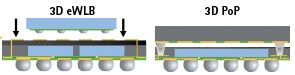

The second configuration is a 3D eWLB Package-on-Package (PoP). Strothmann explained that this is a lower cost option with no topside RDL, resulting in the thinnest package possible. Laser vias are drilled through the mold of the bottom package, forming an interconnect to the first layer of RDL in the bottom. In this way, its possible to stack two eWLBs or on a standard BGA, or any package type with perimeter balls can be attached as the top package. What’s noteworthy, says Strothmann, is that its the only only package in the industry that allows for integrating a processor with stacked memory with
In closing, Strothmann noted that eWLB is not a fit for all applications. TSVs have purpose; namely fine pitch I/0 at 1µm spacing. However, if the fine pitch isn’t necessary eWLB may be your solution, as it is extendable to 5µm line spacing.


