
I didn’t make it to the SEMICON Taiwan SiP Global Summit this year and was hoping to find some coverage by other journalists so that I could at least curate and share the information on the 3D IC Technology Forum. Unfortunately, I didn’t see anything posted on the topic, but Dan Tracy of SEMI was kind enough to share several presentations so I could review and summarize them for 3D InCites. This is not an easy task to do and still get the intended point across, so bear with me and feel free to correct my assumptions if you actually attended this event (or presented there!)
3D IC Supply Chain Readiness
Reminiscent of the ongoing 3D theme of year, the 3D IC Technology Forum focused on 3D IC supply chain readiness, with a keynote delivered by Xilinx’ Vincent Tong. How appropriate, considering Xilinx continues to be 3D’s biggest cheerleader and the only company to actually have shipped 3D interposer products (aka 2.5D).
Tong’s address, titled The Evolution of 3D ICs; leaping Ahead of Moore’s Law to deliver a 6.8B transistor device; describes what Xilinx did by implementing 3D interposer technology in its Virtex-7 2000T. (Note my use of the term 3D interposer vs 2.5D interposer. This is because the term “2.5D does not appear anywhere in this slide deck, and is instead referred to as “3D” throughout. Since the accompanying graphics are ones we’ve all become familiar with under the 2.5D label, I can’t help but wonder if the change in terminology was a result ongoing 2.5D mockery? Personally, I applaud the change. as I’ve never been a fan of the term, 2.5D, but I know for some this is confusing.)
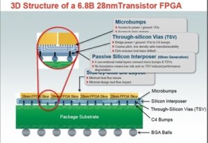
FIgure 1: Xilinx’ 3D FPGA aka: 5D Interposer FPGA (courtesy of SEMI)
In any case, it’s interesting that in the FPGA world, the 2.5D (or 3D) multi-die approach actually achieves cost savings over the monolithic die. Here’s one application where it seems all the goals are realized: increased capacity, high bandwidth, low power die-to-die communications that cost LESS to achieve. Sold on the benefits, Xilinx quickly ramped the second product, a heterogeneous 3D FPGA that place 28g transceivers alongside the logic die on the silicon interposer.
Is his address (ok, in his slide deck) Tong issues a “3D call to action” to develop and evolve standards for: design enablement (modeling and 3D PDKS); manufacturing (DfM rules for TSV, µbumps, aspect ratio and keep-out zones; materials for TSVs and µbump, thermal budget); test (HW, KGD, µbump); Interoperability of silicon between fabs (shipping); and chip-to-chip interfaces.
In his conclusion, Tong says exciting times are ahead for our industry, as economic and technology forces are aligned to enable 3D stacking. Xilinx is already shipping “1000s units to dozens of customers” of its 3D FPGA. Further, he says heterogeneous integration is already here in the form of Xilinx 3D heterogeneous FPGA, which he calls “the world’s highest bandwidth FPGA.” He said the “end game” he notes, will be three distinct technologies; logic, memory and analog.
OSATS/Foundries
Min Yoo, from Amkor Technology Taiwan, presented Amkor’s 2.5D and 3D TSV development update, thereby supplying the OSAT perspective, while UMC’s Kurt Huang offered a foundry perspective. Both provided updates of their respective capabilities, along with their supply chain model.
Figure 2 shows Amkor’s view of TSV production intercepts. Amkor prides itself on its flexibility and adaptability to all the process flows currently being developed including chip on substrate (CoSoS), chip on wafer on substrate (CoWoS); and chip on chip on substrate (CoCoS). And while the company supports wafer backside process in either the fab or the OSAT, their preference is to do it at the OSAT.
 Figure 2: Amkor’s TSV intercepts (Courtesy of SEMI)
Most notable in the capability section of Yoo’s presentation was successful wafer finishing of TSV devices. The company is reportedly cleared to bond up to 40µm front side bumps with “excellent TTV at 2µm. (reportedly on an EV Group bonding system.) In the area of TSV reveal, isolation and passivation, Yoo reports not damage to the silicon liner or tip, and no copper residue on the surface. He also claims successful debonding.
But by far the most compelling message from Yoo came at the end of his presentation in the form a photo. “TSV must succeed or we will face this:” (Figure 3)

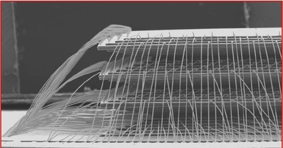
Figure 3: Yikes! that’s a lot of wirebonds (Courtesy of SEMI)
Huang presented UMCs readiness and process flow options for 2.5D and 3D IC. The company claims to have identified and conquered key process issues that affect TSV integrity, such as Cu fill, oxide liner and metal stack. The company’s processes apply to both 2.5D and 3D, and leverages existing CMOS process technology. Huang noted, “After 28nm entry, TSV for 3D may come as a standard option for foundry CMOS logic at 20nm and beyond.” (Figure 4)
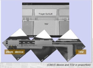 Figure 4: UMC’s 28nm TSV device. (Courtesy of SEMI)
Like the other foundries, UMC is prepared for a number of ecosystem workflow options, with each “service scope” distinguished by middle-end-of-line (MEOL) process inclusion. Workflow optimization may depend on BOM cost, stack recipe and test strategy. Bottom line, once again we’re seeing that there will likely be no one standard approach to the work flow, but that the various options will all co-exist (Figure 5).
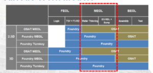 FIgure 5. UMC’s MEOL workflow options (Courtesy of SEMI)
3D Test
Is system level test (SLT) on automated test equipment (ATE) practical at the wafer level for 3D IC processors? This was the question posed by Greg Smith, of Teradyne (Figure 6). According to Smith, increasing coverage at wafer test including SLT coverage is possible for LP-DDR designs, and has been validated to reduce scrap, improve final yield and accelerate time to volume. However, there needs to be more focused efforts on the part of ATE suppliers and device manufacturers to improve ATE capability and device testability. In the case of Wide I/O memory emulation, significant R&D is needed to solve electrical and mechanical challenges before it can be used in production. Yield loss after 3D IC assembly could limit adoption in the most cost-sensitive markets, said Smith.
 Figure 6: SLT at system level vs. wafer level. (Courtesy of SEMI)
Are we there yet?
There’s are fewer and fewer arguments against the transistion to 3D. In fact there are more efforts now than ever to get the proverbial show on the road. But for companies like Xilinx, it’s a no-brainer. A figure in Tong’s presentation sums it up best:


