
Eric Beyne (imec) and I go way back. He’s the Scientific Director of Advanced Packaging Technologies at imec, and ever since my Advanced Packaging days, he’s been a valuable resource whenever I have technology questions about any part of the spectrum of 3D integration technologies. Basically, I can count on Beyne for grounded, technology-based, logical answers devoid of any hype. But lately it seems whenever we cross paths at a conference, we’re both going 100mph in the opposite direction, so there’s a wave a hello and a promise to catch up soon. Soon finally happened this week on a video chat call, where I posed some of my recent burning questions about 3D technology readiness and Eric provided some insight.
From Confusion to Convergence
A sign of progress toward 3D technology readiness, according to Beyne, is the steady migration from confusion to convergence in target applications, technology options (particularly with thin wafer handling) and supply chain role definition. Previously, the multitude of options in the application space for 3D was confusing for materials, equipment manufacturers and foundries, because the technology specs can differ from application to application. Now that the high volume market drivers have been identified (Figure 1), we know we need certain technologies to make them. This has allowed for convergence in 3 different technology areas: namely TSVs, wafer thinning approaches, and wafer stacking approaches. This, in turn, helps the supply chain identify who is doing what (foundry or OSAT) in terms of the front, mid, and back-end of line processes.
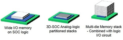 Figure 1: High volume application drivers for 3D ICs. (courtesy of imec)
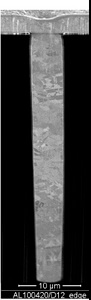 Figures 2a-2c illustrate imec’s perspective of technology convergence. The SEM to the left shows a TSV manufactured imec’ TSV mid process of record: 5µm diameter, 50µm deep, with an overall aspect ratio (AR) of 10. Figure 2b shows examples of a wafer after thinning (50μm), backside passivation and Cu-Nail exposure. Figure 2c shows 3D die μbump stacking – pitch scaling to 20nm.
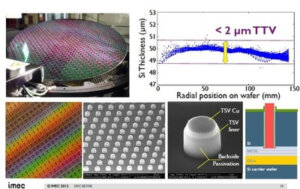 Figure 2b: wafer after thinning (50μm), backside passivation and Cu-Nail exposure.
 3D die μbump stacking – pitch scaling to 20nm.
MEOL Shake Out
I was particularly interested in Beyne’s point of view with various emerging value chain models, which as he noted mainly focuses on who takes on the mid-end (MEOL) processes; the foundry or the OSAT. Beyne’s take is that it will “happen naturally”. It’s clear that TSVs happen in the foundry, and the stacking happens in the OSAT. But wafers can be damaged during thinning, which becomes a liability issue. Additionally, Beyne pointed out, the commercial interests of the parties come into play, for instance when integrating memory on logic. “It’s the IDM that orders the parts, they’ll want to decide who’s doing what. That’s why they prefer multi-sourcing over a one-stop shop,” he explained. So it’s likely that assembly will happen mainly at the OSAT. Beyne agreed that there’s less risk when transporting full thickness TSV wafers than those that are on a temporary carrier or carrier tape, although any of the above can be done. An additional issue with transferring while the wafer is mounted on the temporary carrier is the issue that the bond step would happen at the foundry, while the debond step would take place at the OSAT. This scenario requires close collaboration between the foundry and OSAT to assure that the processes are compatible. For OSATS to take on the backside processing will require them to increase capability levels at the device end. “It’s more complex than just the RDL,” notes Beyne.
Consensus on Temp Bond/Debond
While equipment manufactures continue to promote their capabilities to support a variety of material/process sets for temporary bond and debond (TB/DB) processes to support the variety of applications requiring TB/DB, Beyne says that with regards to volume drivers, there is clear convergence to room temperature debond systems using a peel debond process step (Figure 3). “While it’s not without challenge, it’s clearly the preferred way,” said Beyne. And because of “significant pressure from the industry” to move in that way, the materials suppliers are coming up with more solutions for to support this.
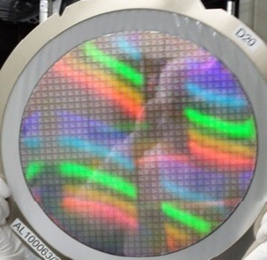 Figure 3: Room temperature peel debonded wafer.

2.5D vs. 3D Interposers
I’ve been noticing what I thought was a shift in terminology from 2.5D to 3D with regard to interposers. I know terminology is important to Beyne, because one key activity he’s involved with as a member of the ITRS Roadmap committee is 3D nomenclature, so I asked him about it. He explained that both terms are alive and well, and explained the difference. 2.5D refers to lower cost packaging interposers that have low-density capability (via connections may require landing pads of 30 or 40µm) require a redistribution layer (RDL) and still need an intermediate interconnect. On the other hand, the technology used for 3D interposers is same that’s used for 3D ICs; the main difference is that the interposer is a passive device. “We use the same TSVs, the same BEOL layers, and the same pitches,” notes Beyne. “the interposer is kind of a chip as well, not just an interposer like a package interposer.” He added that while the interposer is generally a passive device, functionalities can be integrated to make it “lite active” such as with decoupling capacitance.
Silicon or Glass?
Also on the topic of interposers, I asked Beyne’ for his opinion on silicon vs. glass as a substrate material, because there’s been so much attention paid to glass lately. With the caveat that imec works strictly in silicon, he said that although glass is an interesting material, its low thermal conductivity isn’t particularly good for getting rid of heat. If you process (silicon) technology on top of it, the substrate will behave differently. Other downsides: thinning by grinding is more expensive than silicon; through glass vias (TGVs) are still very large and difficult to metallize; special equipment needs to be developed; and while it would be cost effective in large panel format, that would require high-volume production lines. Additionally, PCB manufactures are improving laminate technologies, so glass is facing competition on one side from silicon with micrometer dimensions, and on the other from laminates that already have an established infrastructure and manufacturing base. In Beyne’s opinion, you’re better off going with laminate as an interposer substrate material. “People shouldn’t use interposers just to be in fashion,” said Beyne. “They need a good reason to do so.”
imec’s Continuing Role
Since imec began its 3D program in 2004, it has evolved along with target applications and target technologies. Beyne says the scope of what the technology should look like was developed early on – especially for 3D via-middle. Back then via-last was a popular methodology, and interposers had not yet come into play. Additionally, they were unclear about temporary carriers and bonding. Over the years, via-mid emerged as the technology POR, and via-last has been abandoned for the driver applications (although it’s got a foothold in the CMOS image sensor TSVs). “In many cases, we are focusing on future technology nodes and the impact of TSV on various devices. We’re looking forward. How far can you push the limits?” He explained, citing, as examples, FinFET devices, 14nm devices and the impact of TSV on that, and packaging assembly at 20µm pitch, etc. Additionally, imec has expanded its program partnerships to include fabless companies, 2 OSATS, and EDA vendors; essentially assembling a full ecosystem to take a holistic approach to 3D R&D (Figure 3). For example, as they prepare for the transition to 450mm wafers, they are looking at what this means for 3D and WLP technologies at 450. Up until now, it seems the focus on 450mm tools has been in the front end, where processes are more standardized and repeatable than in WLP, and where the price of tools is several times that of those developed for OSATS. It was good to hear someone is finally paying attention to how this transition will impact the back-end.
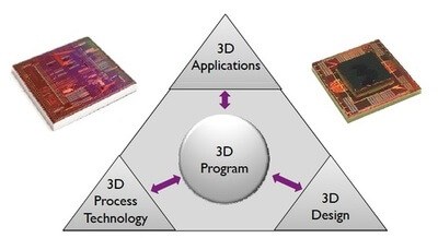 Figure 4: The goal of the program is to concurrently explore and resolve the TECHNOLOGY and DESIGN issues associated with 3D APPLICATIONS DOMAINS. (Courtesy of imec)
The Spirit of Collaboration
In a rare collective appearance, the 3D TSV directors of the three major European research centers —Eric Beyne (imec), Nicolas Sillon (Leti) and Juergen Wolf (Fraunhofer-IZM) — will be presenting at the European 3D TSV Summit, which takes place January 22 and 23, 2013. This first-ever event was organized to demonstrate to the worldwide semiconductor community, the 3D IC capabilities of the European semiconductor industry. Between now and then, I look forward to catching up with Sillon and Wolf, to bring 3D InCites’ readers their perspective on 3D technology readiness. ~ F.v.T.


