
The supply chain business model for manufacturing 3D stacked ICS has caused perhaps one of the hottest debates so far in commercializing 3D semiconductor processes. It’s easy to see why. Beyond the rather obvious question of who will own the liability of damaged devices, there’s a good deal of revenue at stake for those who make the investment in adding capacity for middle end of the line (MEOL) processes, whether they are a pure-play foundry, IDM or OSAT. At last week’s RTI 3D Architectures for Semiconductor Integration and Packaging (ASIP), we heard from TSMC, IBM , and STATS ChipPAC on their manufacturing readiness and arguments for the optimal hand-off point. We also heard recommendations from the research community as well as suppliers.
Douglas Chen-Hua Yu, of TSMC offered 3 different scenarios. In the first foundry/OSAT model, the front end of line (FEOL) and MEOL process take place at the foundry, with the hand-off product being a thinned wafer mounted on a temporary carrier, ready for back-end-of-line (BEOL) final assembly (stacking) and test at the OSAT. The second foundry/OSAT model puts the FEOL processes at the foundry and the MEOL and BEOL processes at the OSAT. The hand-off product in this scenario is a via-mid TSV wafer, still in thick form for easier handling.The final scenario is a ‘single integration’ model where all end-to-end manufacturing takes place at one location: foundry, IDM or OSAT. (The latter is the least likely to adopt this model as it would require cost prohibitive investment in front-end fabs.) Yu identified the single integration scenario as TSMC’s preferred approach. Predictably, IBM’s preferred model is also end-to-end, but performed at the IDM. STATS ChipPAC has added capacity for MEOL and optimized its BEOL for 3D stacking, according to Pendse, targeting the second foundry/OSAT model.
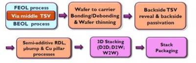
Figure 1: This figure represents imec’s 3D technology process modules for middle end of line processes. Note that debonding actually takes place after backside processes before thinning, but for imec’s development purposes, its included as part of the module for wafer handling. (courtesy, Eric Beyne, imec)
Thin Wafer Handling Options
Handling of ultrathin wafers seems to be the tipping point of where the likely hand off point is. Yu’s argument for keeping all three processes flows, front-end, mid-end and back-end, under one roof is due to the transport issue of wafers post thinning and what he called “the Fed-ex issue”, where this wafers crack or delaminate in the transport process from the foundry to the OSAT. Pendse’s solution was simple: do the hand-off while the wafer is still at full thickness after the front end processes are done, and the OSAT can take it from there, doing the temporary bond, wafer thinning, debond and stacking.
Eric Beyne of imec pointed out that the transport issue is not necessarily confined to transport between companies, but also from facility building to facility building (fab to assembly, for example) within the same company. And while the liability issue is solved by one company handling the processes, the yield issue from potential damage to the thin wafer is no better.
Therefore, finding technology solutions to wafer handling is one way to mitigate at least part of the problem. Beyne said the wafer support system is critical to the success of 3D system integration, however it is not yet fully mature because there is a limited set of materials and equipment available, and most temporary bonding materials are still in the development phase. Imec has prioritized optimizing wafer handling, bond and debond processes. Beyne noted some preferred methods his team has identified.
Temporary bonding to either silicon or glass carriers have been evaluated, and Beyne said that imec has identified silicon carriers as the preferred method because it is the most compatible with post processing. It allows for excellent thickness control – total thickness variation (TTV)- after wafer thinning on the carrier, as well as allowing for low temperature (200-250°C) backside processing. It’s also easy to debond – which has been the more problematic step in the temporary bond/debond processes – at low temperature without melting solder bumps.
Trimming the wafer edge before bonding and thinning to achieve a straight bonded edge post thinning rather than a fragile edge is another critical element in the process identified by imec. This reduces the potential for wafer chipping or cracking, and makes wafer transport post mid-end process while still on the carrier wafer, possible.
Lastly, imec has identified a room temperature peel debonding process as the preferred debond method because the potential to melt solder bumps is not an issue, the thin wafer is bonded to dicing tape prior to bonding, eliminating the need for an interim carrier while protecting the sensitive surface of the wafer backside. However, the TTV capability in comparison to slide debonding has not yet been fully proven, and it requires additional process steps, coating materials, and non-standard tools for surface preparation and cleaning thin wafers on tape. So there are still some kinks to be worked out, even in the preferred method.
Hiroaki Ikeda, of ASET, a 3D research consortium in Japan, offered another research perspective on the temporary bond/debond material, giving thumbs up to the 3M adhesive which uses a laser to ash the adhesive at debond, allowing for easy lift-off.

Where to Bond and Debond
If it is decided that the best hand-off point is post mid-end process, that puts the transport smack in the middle of the temporary bond/debond process. It also requires temporary bond and debond tools to be located at both facilities, which potentially could increase cost-of-ownership (CoO). This once again raises the question, are the mid-end to back-end processes best handled together?
Thorsten Matthias, of EV Group, presented the company’s latest progress in addressing the temporary bond/debond conundrum. One area the company has made great strides in is due to its collaboration with Brewer Science in developing the ZoneBond process. EVG’s contribution (and IP) includes the film frame mounting prior to debonding, and the concept of Edge Zone bonding, in which the center surface of the carrier substrate is treated so that adhesion is minimal there and stronger at the edges. Only low separation force is required for carrier separation once the polymeric edge of the adhesive has been removed buy solvent dissolution or other means dictated by the adhesive being used. Matthias explained the advantage of this is that it decouples the debonding process from the material properties of the adhesive used for the temporary bond. EVG’s temporary bonding and debonding systems are modular, so that if the hand off point is determined to be after temporary bond before debond, the temporary bonding system can live, for example, at the foundry while the debond system lives at the OSAT, theoretically not adding to the cost of ownership (CoO).
Ikeda also pointed out that once a wafer is mounted on the carrier wafer, it can be easily stored for 40 days without issue. Once the chip-to-wafer stacking is done, however, the process moves quickly. For this reason, Ikeda says ASET supports a hand off point after temporary bond with the debond handled at the OSAT.
Conclusion
While these solutions don’t dictate the final determination of hand-off, they at least remove the technical feasibility arguments and/or obstacles, thereby giving the fabless and fablite customers more manufacturing options.
It then comes down to pure business strategy. For foundries to accommodate end-to-end processes for 3D integration requires investment in back-end processes, formerly considered to ‘dirty’ for a foundry, and also requires, as Yu stated, the foundry needs to ‘establish credibility’ in the back-end. Pendse reports that STATS ChipPAC is prototyping 3D stacks beginning with full thickness wafers, and processing through the mid and back-ends without too many issues arising.
At the end of the day, all three models may have a purpose, and depending on the customer and the application, and the market share will be spread to all those willing to risk the investment. Just like the lottery, you can’t win if you don’t play.


