


At SEMICON West 2011, Prof. Rao Tummala of Georgia Tech presented the unique glass and silicon-based 3D Interposer technologies being developed at Georgia Tech, claimed to be simpler and cheaper than 3D ICs with TSV for many mobile and consumer applications at SemiconWest 2011. in his presentation, Tummala discussed the primary differences and challenges between traditional industry’s approach to 3D ICs with TSV versus Georgia Tech’s approach of 3D Interposer with TPV, as illustrated in Figure 1. Tummala calls this patented process the 3D approach in contrast to the 2.5 approach being developed by the industry.
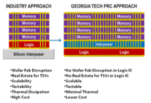
Dr. Tummala explained that the 3D interposer does not require through TSVs in the logic chip. The Georgia Tech 3D Interposers are based on ultra-thin interposers made of either glass or silicon that are the same thickness as the individual chips in the 3D ICs stack: about 30μm. They have through vias that are the same diameter and at the same pitch as TSVs in the 3D ICs, about 5-10μm diameter on 15-30μm pitch.
Unlike 3D ICs with TSV, however, the Georgia Tech approach is scalable, testable, and presents less thermal problems than the 3D IC stacks. It is also cheaper overall. The technology can be applied to 300mm wafers in wafer fabs or 450-900mm panels in package substrate fabs.
3D ICs with TSV are being widely developed around the world for 2 reasons: First, for heterogeneous integration of logic, memory, graphics, power and sensor ICs that cannot be integrated into a single chip. Secondly, 3D ICs with TSVs offer improved electrical performance due to the short interconnect and ultra-high number of TSV interconnections between stacked ICs to address the perceived engineering limits in electrical performance of CMOS ICs beyond 11-16nm and logic-to-memory bandwidth in smart mobile systems. But these benefits come at very high cost and with significant disruption in wafer fabs. Additionally, the 3D stack presents major technical and manufacturing challenges that include testability and yield, scalability, along with thermal and standardized IC interface challenges.
Georgia Tech PRC’s approach is based on an ultra-thin, double-side 3D interposer, made of either low-cost ultra-thin polycrystalline silicon or low-cost ultra-thin glass, not only in 200-300mm wafer form but also in large, 450-700mm panel form. Since the interposer is identical to one of the 3D ICs in the 3D stack in through-via interconnection length and interconnect density, it behaves like a 3D IC stack with TSV. Such an approach does not require TSV in the logic chip; yet it achieves the same bandwidth as 3D ICs with TSVs by virtue of logic IC on one side and memory stack on the other side, interconnected but separated by the 30μm thick interposer.
The 3D interposer approach is scalable by simply attaching chips side-by-side as in the 2.5 approach on both sides interconnected by ultra high I/O redistribution layers (RDL) made of 0.5 to 5μm wiring. The thermal management problems are simplified as well by virtue of separating the logic IC from the memory stack. The single most important benefit of this approach is a cost reduction over wafer and BEOL-based silicon interposers fabricated out of wafer fabs. Contributing reasons for lower cost are many and include large panel size, low cost through-via processes, and low cost RDLs.

Glass has many advantages as an interposer material over silicon; namely ultra-high resistivity and availability in thin and large sizes without having to grind and polish. It is used as a thin and large panel in LCD displays, and thin-film metallization onto these glass panels is well known in plasma displays.
Georgia Tech PRC and its industry consortia partners have demonstrated, for the first time, a very high throughput process for making small holes in glass. Georgia Tech PRC’s approach to 3D silicon interposers is different and unique as it has the potential to achieve equivalent interconnect density at significantly lower cost than traditional Si interposers by use of: 1) Large panel-based substrate up to 450-700mm in size, 2) Cheaper polycrystalline silicon, 3) Low-cost TPV process without DRIE, 4) Low-cost thick polymer liner, and 5) Low-cost, double-side RDL process.
[1] Kumar, G.; Bandyopadhyay, T.; Sukumaran, V.; Sundaram, V.; Sung Kyu Lim; Tummala, R., “Ultra-high I/O density glass/silicon interposers for high bandwidth smart mobile applications,” 2011 IEEE 61st Electronic Components and Technology Conference (ECTC), pp.217-223, May 31 2011-June 3 2011.


