

NHanced Semiconductors News
The SMTAI Conference to Feature a Presentation by NHanced Semiconductors VP Charles Woychik on Hybrid Bonding in Chiplet Architectures
Woychik’s presentation will highlight the role of hybrid bonding in supporting die-to-wafer and wafer-to-wafer in delivering high-density, low-latency interconnection technology...
INFIERI Summer School Program Features NHanced Semiconductors President Robert Patti Presenting Advanced Semiconductor Architectures for Future Memory Systems, AI, & HPC
The 8th Edition of the Intelligent Signal Processing for Frontier Research & Industry (INFIERI) Summer School was held September 1...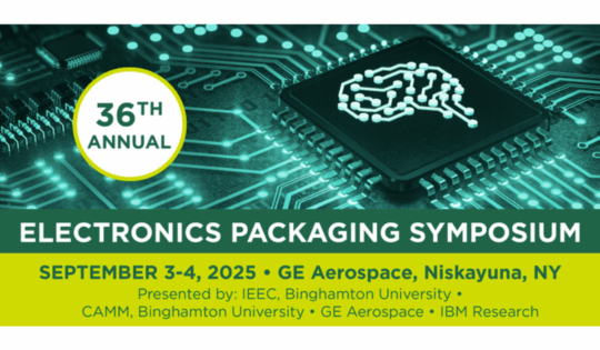
NHanced Semiconductors & University of Florida to Present Chiplet Paper at 36th Electronics Packaging Symposium Held at GE’s Aerospace Research Campus
The paper presents a comprehensive technical roadmap and process assessment of using hybrid bonding to integrate fine pitch chiplet architectures ...
NHanced Semiconductors VP Charles Woychik to Deliver Keynote at SMTA’s Symposium on Counterfeit Parts & Materials in College Park, Maryland
Woychik’s address will highlight the critical role of advanced packaging technologies in the evolution of the U.S. OSAT industry to...
NHanced Semiconductors President Robert Patti to Detail “Foundry 2.0” at SEMIEXPO Heartland
New manufacturing model extends Moore’s Law via advanced packaging, employing a range of 3D IC processes for Foundry 2.0 At...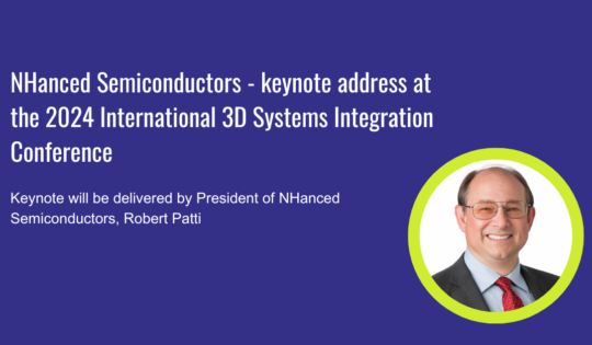
NHanced Semiconductors President Robert Patti to Deliver Keynote at IEEE 3DIC Conference in Sendai, Japan
Patti’s keynote address will highlight the role of advanced packaging in extending the progress of Moore’s Law in semiconductor development...
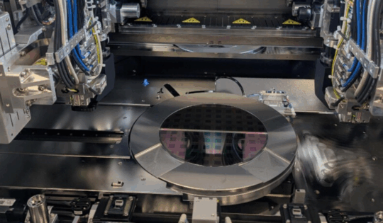
NHanced Semiconductors Announces Delivery of the First Next-Generation Hybrid Bonding System from BE Semiconductor Industries
The Besi Datacon 8800 CHAMEO ultra plus advanced hybrid bonding system delivers faster throughput, enhanced accuracy, and superior warpage control for room temperature...NHanced Semiconductors Opens Leading-Edge Advanced Package Assembly Facility, Reinforcing Indiana’s Position as a Major Semiconductor Hub
U.S. Senator Todd Young (R-IN) and NHanced Semiconductors President Robert Patti, at the ribbon-cutting at the Odon facility, announce new...
New Advanced Packaging Facility Coming To Indiana
Nov 21, 2022, saw the groundbreaking for WestGate One, a semiconductor campus that will house the first fab in the...
NHanced Semiconductors Launches High-Tech Nexus in Indiana
Will leverage next generation technologies, spur workforce development, seed small businesses NHanced Semiconductors announces a new office in the Westgate...