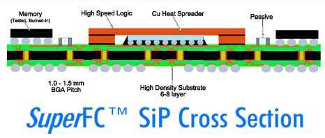
The challenge of designing smaller, cost-effective systems that require additional processing and performance power led to 3D chip stacking of bare die and a new approach to packaging known as SiP (systems-in-package), also known as multi-chip modules (MCMs). The benefits of MCM/SiP package technology include the ability to achieve greater functionality in a reduced time-to-market window that cannot be accomplished through direct silicon integration or ASIC development. Along with the many benefits of the SiP approach came new design challenges. This paper focuses on a common occurrence in systems companies: how to design SiPs that are optimized for their target PCBs.
MentorPCB
The Bio hasn't been uploaded yet
Related Category Posts
Affordable and Comprehensive Design-for-Test of 3D Stacking Die Devices
Feb 27, 2024
The semiconductor industry has made great strides in ASIC technology...
An Organic Package Designer’s Guide For Transitioning to FOWLP and 2.5D Design
Nov 28, 2023
Numerous package designers possess extensive hands-on experience in crafting organic...
Chiplets and HI are Revolutionizing System Design Analysis
Jun 26, 2023
In electronic product design, solely relying on process shrink as...
Related Tag Posts
Driving Collaboration Across Design Teams to Optimize 3D-IC Designs
Jun 13, 2023
Editor’s Note: Bob Smith, executive director of the ESD Alliance,...
The Rise of Organic and Glass Substrates
May 30, 2023
If you are designing a heterogeneously integrated, multi-die, high-performance device...
SEMICON West Smart MedTech Panel: Design Verification in the Supply Chain
Jun 09, 2022
All electronic products begin with design be it a single...