Wafer and panel-level packaging (WLP/PLP) offers technical and business advantages, compared to traditional IC packages. These cost-effective packaging solutions attracted more than 800 industry experts to the International Wafer Level Packaging Conference (IWLPC 2018) in San Jose’s DoubleTree Hotel at the end of October.
In case you were wondering, a multi-die WLP design, created with the tools discussed here, is already in high-volume production. iPhones 8, X and Xs enjoy the small form factor, low power and high performance enabled by TSMC’s version of WLP, “InFO”.
Representing Team EDA
In addition to many manufacturing experts, several EDA experts from Cadence and Mentor also attended IWLPC. Three of them as presenters: Wally Rhines, CEO Emeritus, Mentor, a Siemens Business, gave one of three keynotes; and Mentor’s Keith Felton and Bill Acito, Cadence, presented during the EDA session. This blog post uses slides from Keith Felton’s presentation, developed jointly with his colleagues Kevin Rinebold and John Ferguson at Mentor. Other slides are from Bill Acito. He works on John Park’s team at Cadence.
Both presentations were very well attended. Manufacturing experts occupied every chair in the large Cedar conference room. It looks like the time is right, to further increase dialog and cooperation between the manufacturing and design community.
Revisiting the Challenges
Before I dive into Acito’s and Felton’s individual IWLPC presentations, allow me to recap:
- The most important roles of IC packaging: Mechanical protection of the die(s), thermal management, supplying power to the die(s), conducting signals between die(s) and to and from the board as well as integrating passives.
- Basic IC packaging problems: As pin counts and signaling frequencies continue to increase, maintaining signal integrity (SI) is getting much more challenging. In addition, designers need to pack more functionality, at higher frequencies, into a package, leading to increased power density. Managing the integrity of power supply (PI), as well as thermal and mechanical stress, is getting more difficult. Also, the optimal placement of embedded passives is becoming more critical. Last, but not least, customers demand increasingly shorter lead-times and more complex (sub)system solutions at lower and lower cost.
Enough said about the challenges EDA can contribute to solving in advanced IC package design. Let’s get to the key messages Mentor’s Felton and Cadence’s Acito conveyed.
What the EDA Experts Say
Both presenters demonstrated that their companies have developed solutions to make package designers’ lives easier and allowed me to illustrate this blog with a few of their slides, about features and benefits of their planning, design and verification tools and flows.
Figure 1 highlights the package designers’ key problem: They are stuck in the middle! Package designers often face completed die and board designs and have to unscramble the interconnects in-between.
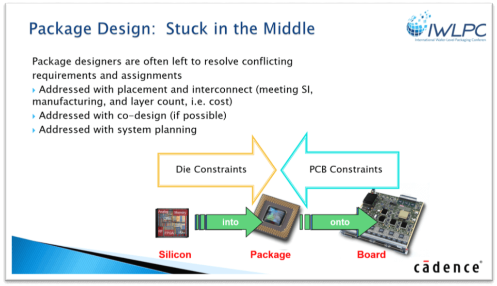
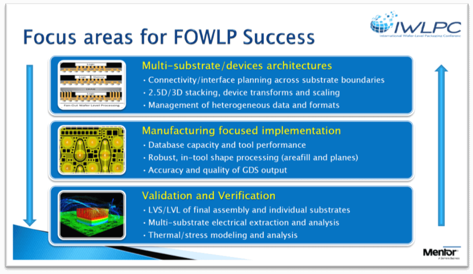
Figure 2 shows key considerations for the planning, implementation and verification steps. He also emphasized that Mentor’s tools can manage very large databases for these steps. He mentioned that package designers typically start work for improving/modifying an existing design with step 3, validation and verification.
They use the system-level netlist to check, e.g. functionality, timing, and geometry fit, before going to step 1, where they use Pathfinding methodologies and system-level models, to analyze and optimize the design on a high level, before starting step 2, the actional implementation.
Investing time and efforts in the architecture stage clearly minimizes the number of required changes further down in the design process. Felton also emphasized that Mentor’s tools simplify the typically required iterations between these three major design steps.
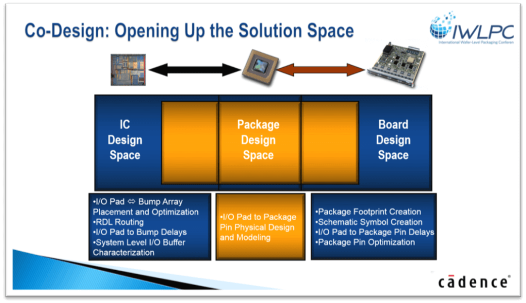
Acito reminded his audience that the ideal, and most promising approach, is to initiate a die-package-board co-design methodology at the beginning of every new project. Designing die, package and board in conjunction allows for trade-offs between them, opens the solution space, and leads to globally optimized design solutions (Figure 3).

Because thermal management is easier in interposer-based (a.k.a. 2.5D) designs, versus 3D-ICs (vertically stacked dies), interposer designs are needed today. Felton presented Mentor’s basic interposer design steps (Figure 4).
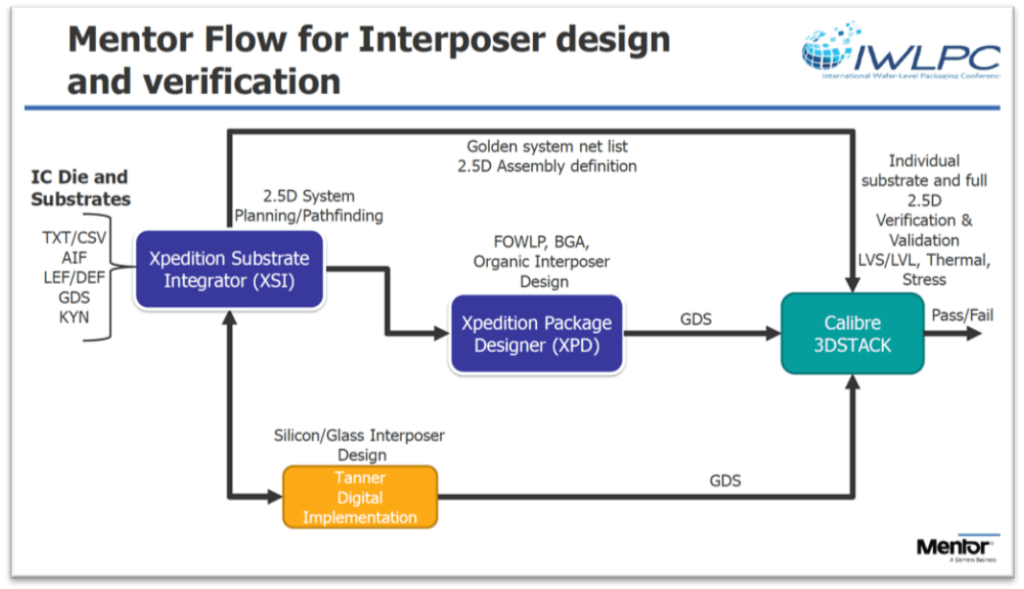
Figure 5, from Bill Acito’s presentation, gives a global picture of Cadence’ co-design environment and shows that die-package-board co-design employs a number of tools and requires iterations between adjacent and other design steps, to find the best solution.
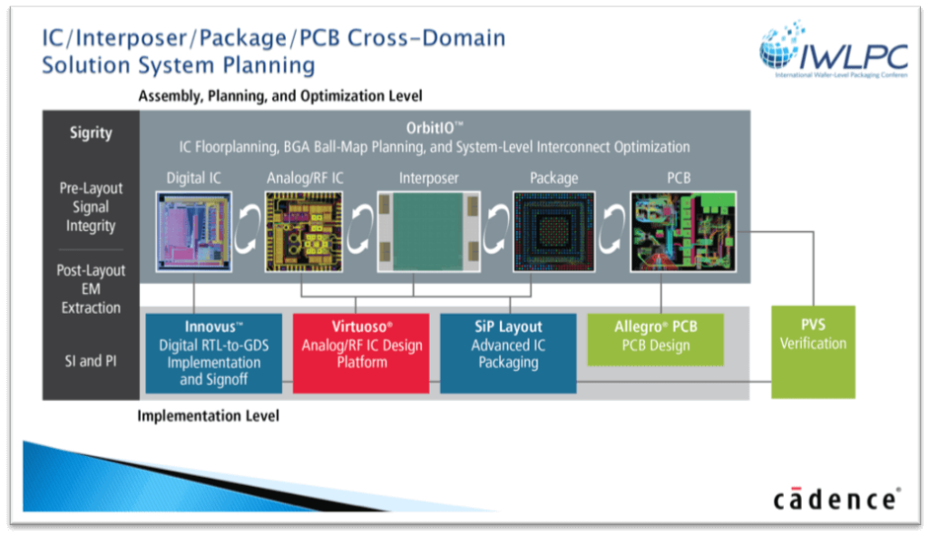
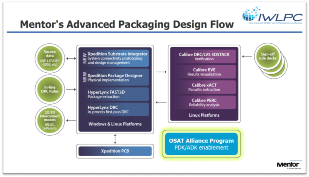
Figure 6 outlines Mentor’s advanced packaging design environment. The green circles show which input data the tools require. With the OSAT Alliance Program box on the bottom right, Felton referred to the partnerships between Mentor’s EDA developers, OSATs and their suppliers.
Only if the design tools receive accurate and up-to-date inputs that specify materials characteristics (e.g. CTE), equipment capabilities (e.g. min resolution) and manufacturing flow specifications (e.g. processing temperatures) can the tools assist package designers meaningfully in the creation of reliable and cost-effective solutions.
Focus on WLP/PLP
Both presentations’ primary focus was WLP/PLP. Why? Because, this relatively new packaging technology allows to establish best design practices now, before every package designer defines his/her own way of getting the job done… and then becomes reluctant to change. Also, this focus is justified, because WLP/PLP promise to gain a significant share of the market. They offer good thermal management and PI / SI advantages versus today’s flip-chips. Above all, WLP and especially PLP promise significantly lower high-volume manufacturing cost, compared to traditional solutions.
What’s Next?
The annual MEPTEC Symposium, to be held at SEMI in Milpitas, CA, on December 5, will outline market trends, latest innovations and again encourage closer cooperation between designers and manufacturer. Please join me there!
The Electronic System Design Alliance, a SEMI strategic association partner, recently announced the ES Design West Debut in Conjunction with SEMICON West 2019. This EDA/Design focused event will be co-located with SEMI’s manufacturing-centric conference, to bring – on a very large scale – design and manufacturing experts closer together. I look forward to meeting you there ~ Herb