ECTC 2025
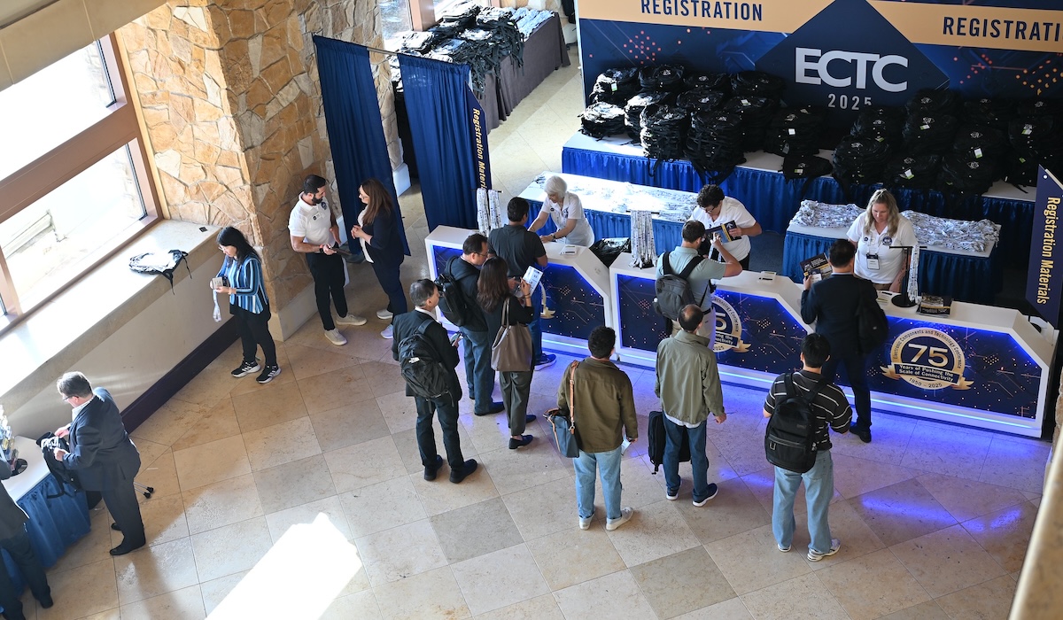
The 75th annual IEEE Electronic Components and Technology Conference (ECTC), was held this year in Dallas TX over memorial day week. It featured:
- 2,500+ attendees
- 390 technical papers presented in 36 oral and 5 interactive presentation sessions.
- 16 professional development courses
- Industry support included 51 corporate sponsors and 138 booths in the exhibit hall
Let’s take a closer look at one of the key silicon bridge papers presented by Samsung at the conference.
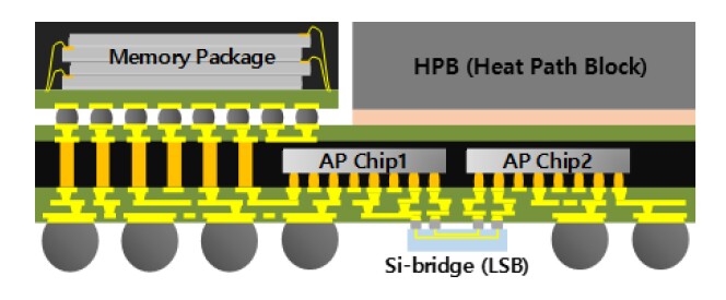
Samsung Fan Out Package Chiplet interconnect Using Land-Side Bridge
A key challenge in chiplet design is the interconnection of multiple chiplets within the package. Conventional system-in-package (SiP) designs typically interconnect chips use copper traces within the organic substrate or copper redistribution layers beneath the chips. State-of-the-art chiplet interfaces, such as Universal Chiplet Interconnect Express (UCIe), have increased the number of I/O signals and minimized interface latency.
Therefore, Samsung investigated improved chip-to chip interconnection technology beyond existing RDL processes. In this paper, they propose a new Fan-out Package (FOPKG) structure for chiplet interconnection that maintains the existing FOPKG RDL structure. The figure below illustrates the proposed multi-chip FOPKG architecture, which uses a land-side bridge for chiplet interconnection. A land-side bridge, mounted on the ball lands, connects AP chip1 and AP chip2. Because the fine-pitch connections required for chiplet interconnection are routed using the land-side bridge (LSB) structure, the FOPKG RDL structure can maintain the same three-layer stack up and 5/5 μm line/space as before, resulting in what they feel is a more cost-effective solution. Furthermore, they claim that it is more efficient in terms of simplified integration process and higher yield, compared to a silicon interposer.
Samsung reports that interconnecting a UCIe x64 advanced package, a common chiplet interface, using RDL layers would require a nine-layer RDL structure with 2/2 μm line/space. Using high-bandwidth D2D interconnections with conventional RDL processes increases the number of layers and cost.
Die-to-die (D2D) interconnection using silicon interposers has become increasingly prevalent. The silicon process enables finer signal pitch (1-2 μm), denser signal routing, support for more I/Os, and improved signal integrity characteristics. The silicon bridge, such as Intel’s EMIB, is a D2D interconnection structure that leverages the silicon process to provide denser signal routing within a smaller silicon slice. In this paper, Samsung proposes the Land-side Bridge (LSB) structure, which is mounted on the land side of the package, similar to a Land Side Capacitor (LSC). This LSB structure results in a reduction in the number of RDL layers compared to existing RDL designs and enables the transmission of higher speed signals due to the finer pitch of the silicon process.
They used UCIe Specification 1.1 to verify the signal integrity (SI) of the chip-to-chip interconnections within the chiplet structure. focusing on three key metrics: crosstalk, insertion loss, and eye opening. They claim to have achieved excellent SI performance with ample margin across all metrics.
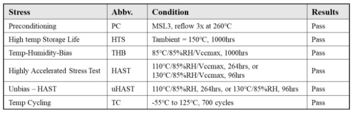
The assembled test vehicles were subjected to a range of environmental and stress conditions, including Preconditioning (PC), High-Temperature Storage (HTS), Temperature Humidity-Bias (THB), unbiased Highly Accelerated Stress Test (uHAST), HAST and Temperature Cycling (TC). The results of these tests, detailed in the table below, demonstrate that the LSB structure passed all reliability requirements, exhibiting no delamination within the RDL layers and no cracking in the joints.
A land-side bridge (LSB) structure utilizes existing RDL processes on the chiplet side and a more advanced silicon process for the bridge itself to achieve high-performance interconnects.
The LSB is mounted on the land side of the chiplet, similar to a Land-Side Capacitor (LSC), simplifying integration and providing greater design flexibility than conventional RDL processes, particularly in terms of trace routing.

Micron Expansion in the US to Include HBM Packaging Capacity in Va.
In IFTLE 634 we discussed Microns announced production expansion of capacity in the US. We now have more info on this expansion.
Micron has announced a renewed U.S. buildout strategy that expands investment plans to $150MM, builds an HBM packaging facility in Virginia, and invest some $50B in R&D. Micron’s first new U.S. fab in years will begin operations in the second half of 2027, the company revealed this month.
Following the enactment of the CHIPS and Science Act in August 2022, Micron unveiled major plans to build new fabs worth over $115 billion in Idaho and New York with the aim of building 40% of its DRAM products in the U.S. over the next decade. Under the new plan, Micron projects investing $200B in U.S.-based memory production and R&D over the next 20+ years, with support from the U.S. government.
The effort includes $150B for manufacturing and $50B for R&D. The new plan envisions two leading-edge DRAM fabs in Idaho, a site with four fabs in New York, and an HBM packaging facility in Virginia.
Micron says it is set to expand its facility in Manassas, Virginia which currently manufactures memory chips for automotive, aerospace, defense, and industrial applications. After the upgrade, the fab will gain capacity as well as advanced packaging capabilities to assemble HBM memory stacks in the U.S. However, Micron will only add HBM capability to its Virginia plant after it ramps up production of enough DRAM wafers in the U.S. at its fabs in Boise, Idaho. That said, expect Micron to build HBM5 or HBM6 in the U.S.
For all the latest on Advanced Packaging stay linked to Insights From the Leading Edge (IFTLE) ……………………………..