
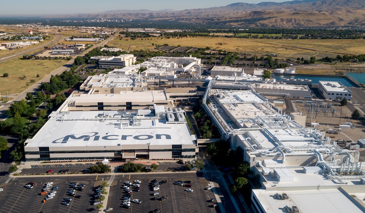
Micron Expands Investment
In IFTLE 631 we asked whether any other companies would up their own investments to onshore chip production in the US after TSMC announced further major cash investment. Now we have learned that Micron, the sole U.S.-based manufacturer of advanced memory chips, has announced $$ additions to their previously announced CHIPS Act investment.
The overall investment includes construction of a second chip fabrication facility in Boise, Idaho, modernizing its Manassas, Virginia, facility and onshoring production of its advanced DRAM technology from Taiwan for the first time.
This facility will reportedly improve supply chain resiliency for U.S. automotive and industrial markets and the defense industrial base. Micron’s expanded $200 billion investment also includes up to two additional fabrication facilities in New York.
Previously, the Department of Commerce awarded up to $6.165 billion in CHIPS Act direct funding on December 10, 2024, as part of Micron’s commitment to build three fabrication facilities in Idaho and New York. Today’s expanded investment of $200B by Micron is accompanied by up to $275MM in incremental CHIPS Act direct funding.
The move, aimed at strengthening America’s domestic chip supply chain, represents an additional $30B beyond Micron’s previous investment commitments.
The company said it will keep aside $150 billion for manufacturing amidst U.S. President Donald Trump’s push to onshore the production of semiconductor chips. The company will also dedicate about $50 billion to R&D, Micron said.
The company said the Idaho sites will help accelerate the development of high-bandwidth memory (HBM) products and allow it to meet rising global demand for DRAM chips, which are essential in AI and high-performance computing (HPC).
TSMC readies COPOS Mass Production
TSMC’s CoWoS is reportedly moving ahead with its Chip-on-Panel-on-Substrate (CoPoS) technology amid strong AI demand. TSMC’s first CoPoS pilot line is set for 2026, with mass production targeted for 2029.
Reports are that NVIDIA will likely be the first big customer for TSMC’s CoPoS.
According to the reports, TSMC’s CoPoS is essentially a square-panel evolution of CoWoS-L and CoWoS-R, replacing the traditional round wafer with a rectangular substrate. Measuring 310 x 310mm, the rectangular design offers more usable substrate space than traditional round wafers, boosting output and theoretically cutting costs.
TSMC’s AP7 site in Chiayi is shaping up as a key hub for next-gen advanced packaging. The campus, planned in eight phases, will start large-scale CoPoS production in phase 4.

The first phase (P1) of AP7 will reportedly serve as a dedicated WMCM (multi-chip module) base for Apple, while phases 2 and 3 focus on ramping up SoIC production. Notably, CoWoS production is not planned for AP7 and remains at AP8.
This extra surface makes it possible to integrate additional high-bandwidth memory stacks, multiple I/O chiplets and compute dies in a single package. Unlike wafer-level packaging (WLP), PLP assembles components on large, rectangular panels, delivering higher throughput and lower cost per unit. Systems with PLP should allow faster iterations vs WLP.
TSMC will establish a CoPoS pilot line in 2026 at its Visionchip subsidiary. In 2027, the pilot facility will focus on refining the process, to meet partner requirements by the end of the year. Mass production is projected to begin between the end of 2028 and early 2029 at TSMC’s Chiayi AP7 campus. That site, chosen for its modern infrastructure and ample space, is also slated to host production of multi-chip modules and system-on-wafer technologies.
NVIDIA is expected to be the launch partner for CoPoS. The company plans to leverage the larger panel area to accommodate up to 12 HBM4 chips alongside several GPU chiplets, offering significant performance gains for AI workloads. At the same time, AMD and Broadcom reportedly will continue using TSMC’s CoWoS-L and CoWoS-R for their high-end products. Beyond simply increasing size, TSMC nots that CoPoS and PLP may combine with other emerging advances, such as glass substrates and silicon photonics to generate new advanced packaging technologies. If development proceeds as planned, the first CoPoS-enabled devices should reach the market by late 2029.
Fan-out panel level packaging (FOPLP) and CoPoS both utilize large panel substrates for packaging, but they differ significantly in architecture and application, particularly in the use of interposers.
FOPLP is a packaging approach without an interposer, where chip dies are redistributed directly onto a panel substrate and interconnected through redistribution layers (RDL). This results in advantages such as lower cost, high I/O density, and flexible form factor, making it suitable for applications like edge AI, mobile devices, and mid-range ASICs where integration density is moderate.
In contrast, CoPoS incorporates an interposer, which enables higher signal integrity and stable power delivery—especially important when integrating multiple high-performance, high-power dies, such as GPU and HBM. TSMC reports that the presence of the silicon interposer makes CoPoS more suitable for high-end AI and HPC systems that require large-area packaging and high-speed data transmission.
For all the latest in Advanced Packaging stay linked to IFTLE………………………


