


The 2021 3D InCites Awards program recognized industry-wide contributions in the development of heterogeneous integration and 3D technologies. We expanded our scope of coverage, adding a special focus on sustainable manufacturing efforts, as well as diversity equity and inclusion (DEI) with two special award categories. Like every other awards event in the past year, we had to adjust how we celebrated the winners of the 2021 3D InCites Awards. Because we can’t gather in person, we asked our winners to send us an acceptance quote and video clip saying a few words about their achievement. We compiled them here on this Winner’s Circle page.
Please join us in officially congratulating the winners of the 2021 3D InCites Awards. We look forward to a time when we can gather in person once again to celebrate!
The Circle
Sustainability Award:ASE Group
We are truly grateful to have been selected as the winner of 3D InCites’ first Sustainability Award, especially given the other incredible finalists that likewise are laser-focused on doing all that can be done within our individual and collective power to make the world a better, safer, and healthier place for generations to come.Patricia Macleod
3D InCites Sustainability Award, chosen by committee, is given to a company that sets an example through best practices for sustainable semiconductor manufacturing.
The winner, ASE, earned high marks for its commitment to reducing absolute scope 1 GHG emissions and upgrading its water reclamation facilities. The company is also working with its supply chain to address scope 3 emissions. ASE Technology Holding Co. earned a position on the CDP’s A list for both climate change and water security for 2020, the only finalist to achieve the top grade in both categories. It is increasing the recycling of both hazardous and non-hazardous waste and has embarked on cross-industry partnerships to find more reuse opportunities.

SemiSister of the Year:Lam Research
It is my pleasure to accept the 3D InCites SemiSister Award on behalf of Lam. We are very pleased to be recognized for our diversity and inclusion efforts.
At Lam, our vision is for every person to feel valued, included, and empowered to achieve their full potential. These efforts are enabled by senior leadership to ensure the highest level of attention is devoted to our inclusion and diversity goals and aligned with our Core Values.Antoinette Hamilton, Head of Diversity and Inclusion at Lam Research
Our 3D InCites SemiSister Selection Committee weighed the five finalists in the area of diversity, equity, inclusion, access, and leadership. Additionally, did they adhere to the environmental, social, and governance (ESG) criteria that socially conscious investors use in their screening process? Bonus points were given to organizations with a purpose-driven mindset, that is instilled in their employees to support the community.
While all five finalists demonstrated excellence in most of the criteria, the committee felt strongly that Lam Research sets the standard with strong messaging around DEI and ERG. Women are well represented on its board and leadership team. Lam is very transparent about its DEI efforts, and the company has a veteran’s program as part of its hiring/onboarding process.
Device Manufacturer of the Year:3D Plus
3D stacked "Space Camera" Device which was applied for 2020/2021 Mars mission Perseverance
Perseverance integrates numerous 3D PLUS’s highly reliable components such as volatile and non-volatile memory modules (SRAM, SDRAM, NAND Flash, NOR Flash and DDR2), Latch up Current Limiters, Interfaces, as well as our unique CMOS space qualified camera head. Embedded in multiple instruments of the rover, 3D PLUS products offer high reliability, radiation tolerance and weight saving thanks to our unique stacking technology that allows a high level of miniaturization.
Device Technology of the Year:AMD/EPYC Processor
For EPYC, AMD partitioned the design to put the CPU functions that would benefit most from the next node (7nm) while leaving analog and I/O blocks for a less advanced technology. It all makes perfect sense. The analog circuits simply do not benefit from scaling transistors or interconnect pitches. It is even more striking to consider the I/O themselves with bump pitches for getting signals off chip scaling very slowly compared to the digital circuits. AMD calculated an additional 10% of silicon real estate required for the die-to-die communication blocks, redundant logic and other unnamed add-ons to enable the chiplet design compared to a hypothetical monolithic EPYC chip. The total die cost of the multiple chiplets saved 41% compared to AMD internal estimates for the monolithic processor.
Engineer of the Year:Severine Cheramy
Severine is known worldwide for her work at CEA-Leti, developing processes, most notability wafer bonding processes, that furthered the course of 3D integration. She first joined CEA-Leti in 2008 as project lead. In 2011 she became 3D integration Lab Manager, and in 2017, became responsible for 3DIC integration strategy and business development at CEA-Leti. She also directed the Institute of Technological Research (ITR) 3D integration program, ITR Nanoelec As part of her work at Leti, she presented multiple papers at IMAPS and IEEE events, and organized an annual event to promote the work ITR Nanoelec. Chéramy holds an engineering degree in material science. She spent more than eight years at GEMALTO, a leading smart-card company developing technologies for secure solutions such as contactless smart cards & electronic passports.
Equipment Supplier of the Year:Evatec AG
We are extremely proud of our team at Evatec for all their hard work developing the tool, and for being selected by 3D InCites’ readers and judges as the winner of this year’s award. Thanks to everyone who voted for us.
Large area cluster tool for single panel processing – introduced in 2017 – already volume production-proven by major IDMs and OSATs with panel sizes up to 550mm. The latest version now offers the capability for substrate sizes up to 650mm. It integrates degas, etch, and deposition capabilities for Advanced Packaging applications including Fan-Out Panel Level Processing (FOPLP) and advanced IC-Substrate manufacturing. For instance, Samsung Electro-Mechanics Co. Ltd. worked with Evatec to solve challenges in Fan-out packaging technologies for the successful volume production of their FOPOP for Samsung’s GALAXY watch (package size reduced 65% of the previous package size, RDL L/S at 7/8µm with a joint pitch to memory of 150µm. Semco underlined the success factors: "With Evatec and their solution for a panel level sputtering tool we found a strong reliable partner to help us solve the 3 main challenges we needed to address: Warpage of the substrate, Fine pitch RDL, and Process reliability. Learn More
Herb Reiter Design Tool Provider of the Year:Deca
In 2020, Deca Technologies introduced Design During Manufacturing (DDM) capabilities to support its licensees and partners in implementing Adaptive Patterning™ (AP). AP Live, a cloud-based solution that eliminates the need for dedicated on-site hardware and software, allows customers to gain early access to AP and experience its power for improving yield, scaling technologies, reducing cost and enhancing performance. To effectively implement AP Live, Deca created a complete ecosystem comprising three components including AP Studio, AP Connect, and AP Engine. AP Studio is integrated into EDA partner software to provide a best-in-class design environment for heterogeneous integration, system-in-package (SIP) and chiplets. AP Engine efficiently performs real-time design on every package as it flows through the manufacturing process. AP Connect software is integrated directly into high-volume manufacturing equipment, so it connects with AP Studio design systems and the AP Engine to make tools AP-ready. When it’s time for high-volume production, the same AP Live system is proven ready for on-site deployment, without any change to the interface or results.

Material Supplier of the Year:Plan Optik
We are very proud and overjoyed that we’ve been selected as the winner of the prestigious 3DInCites award in the category "Material Supplier of the year"! Many thanks to the judges and everyone who voted for us! In addition we would like to thank the whole 3DInCites team for their great work!Markus Wagner, Marketing & Communications
Plan Optik AG is the leading manufacturer of patterned wafers when it comes to technology. Since more than 40 years, Plan Optik supplies glass materials in sectors such as consumer electronics, automotive, aerospace, chemistry and pharmaceuticals. Plan Optik’s high quality wafers are used as essential components for numerous applications in MEMS and Sensor technology. The wafers made of glass, glass-silicon compounds or quartz materials are available in sizes up to 300 mm diameter with application-specific structuring and complex material combinations.
To serve the high demand of glass wafers with fixed specifications more quickly, Plan Optik has founded the brand Wafer Universe to provide off the shelf products. Therefore, every customer can be served with glass wafers in respond to its needs – simple and fast.
Process of the Year:Veeco
We'd like to extend a big thank you to 3D InCites and the judges for recognizing the potential of Veeco's approach to wet wafer processing for 5G applications. In addition, we'd like to thank everyone who voted for our process capabilities. We look forward to continuing to enable future generations of global megatrends, such as 5G, AI, AR/VR and other advanced electronic devices.Kevin Long, Sr. Manager, Marketing & Communications
Although COVID-19 stalled the 5G rollout, 2020 was a pivotal year for process development at Veeco. The company’s proprietary WaferStorm® wet processing technology found its ideal use in 5G applications. For a technology that was far ahead of its time, WaferStorm proved critical in 2020 because it vastly improved upon conventional processes. By doing so, it helped make 5G a reality during a deeply unprecedented era.
WaferStorm’s wet processing approach uses immersion, followed by a high-pressure spray that’s tough on photo resist. It uses 5x less chemistry than conventional processes while doubling throughput over single wafer approaches. It’s unique processing application for metal liftoff and photo resist strip applications offer a cost-effective alternative to etch processes that can damage underlying substrates. Chambers are stackable for a compact footprint while still supporting high volume needs.
As the 5G revolution accelerates, Veeco is transforming processing.
Research Institute of the Year:imec
I am honored to accept the 2021 3D InCites Award for Research Institute of the Year. This is a great recognition for the research of the imec 3D System Integration team and it is also a great encouragement to continue our research to advance the field of heterogeneous system. We are grateful to all the companies that support and contribute to our 3D System integration program and allow us to continue to perform this research.Eric Beyne, Director 3D System Integration Program at imec
In the Imec view, there are three key technology elements for 3D integration:
Through-silicon-via (TSV)
Die-to-die, die-to-wafer stacking & interconnect
Wafer-to-wafer bonding & interconnect technology.
Imec's research is showing good promise for scaling TSVs. However, vias in commercial products have remained static. The problem is the “interconnect gap.” The microbump has not caught up to the point where the TSV can be fully utilized. More aggressive scaling is necessary.
Teams at Imec have been working on improving bump density. Imec's work showed solder bump pitches down to 7µm with thermocompression bonding. The SEM images showed a technology demonstrator with four stacked die with 7µm pitch TSV bumped and interconnected. Clearly, Imec wants the industry to realize the opportunities and get microbumps up to speed with TSV technology.
Start-up of the Year:MZ Technologies
We are humbled and honored that Genio™ is recognized by a forward-looking technology advocate like 3DInCites. Their membership includes some of the biggest names in the technology space and I’m grateful that they have recognized the accomplishments of our brilliant engineering team.
MZ Technologies has launched a design tool for the 3D co-packaging of chips and chiplets down to the PCB level. Genio supports the design of 2D, 2.5D, and 3D multi-component systems and operates across multiple levels including die, chiplet, silicon interposer, package, and PCB. There are three different versions specifically for 2D, 2.5D, and 3D design. The tools use standard design data formats to integrate with existing commercial EDA tools and this allows dedicated plug-ins to integrate into non-standard custom EDA flows. It has a graphic interface that provides an interactive 3D visualization of the complete system.
Monozukuri was founded in 2014 by a team of EDA IC and package co-design engineers with the intention of building 3D EDA technology from scratch that can deal with the I/O planning and optimization phase of the physical implementation of complex 2.5D and 3D ICs. The company's founder and CEO is Anna Fontanelli.
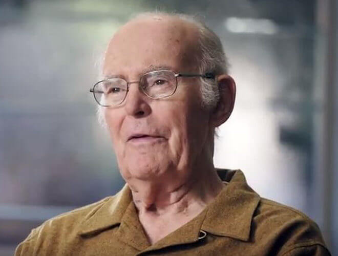
Lifetime Achievement Award:Gordon Moore
In 1965, Gordon Moore wrote a very short paper, four pages, on what has become known as Moore’s Law. On the third page he said, 'It may prove to be more economical to build large systems out of smaller functions which are separately packaged and interconnected.’ And lo and behold, here’s where we are with the advanced packaging technology that we have today. And so, in a way, it’s just a continuation of what Gordon asked us to do.