
The 3Dblox Open Standard Continues to Evolve
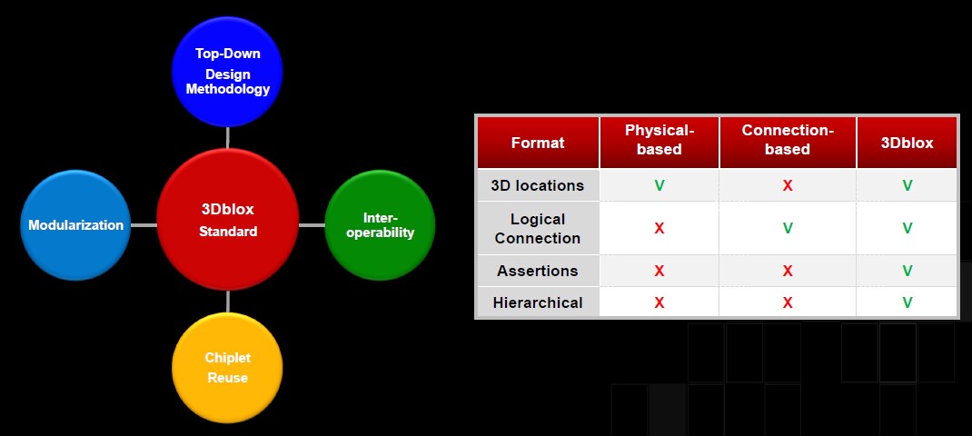
Introduced in 2022, the 3Dblox open standard has provided EDA vendors with a pathway to model the essential physical stacking and logical connectivity information for 3D IC designs in a single format. 3Dblox reportedly simplifies 3D IC design by providing a complete view of physical and logical connectivity.
In general, the industry has lacked common protocols in the early phase of chip-package co-design. The 3Dblox Common Constraint Format bridges the gap by providing a formal definition of the needed constraints to facilitate precise communication between teams and ensure the rapid convergence of package and integration rules.
Since its inception, the 3Dblox standard has undergone several updates. In 2022, 3Dblox implemented a modular approach for the representation of all 3D IC architectures. In 2024 3Dblox focused on prototyping feasibility for early architecture exploration. The latest version of 3Dblox focuses on “…tackling large 3D IC design with early planning capabilities”.
The 3Dblox committee has announced its plans to make the 3Dblox standard publicly available through IEEE (Figure 1).
.
Dr. L.C. Lu, TSMC fellow and vice president of Design and Technology Platform noted “…we’re enabling customers to harness TSMC’s leading process and 3DFabric technologies to reach an entirely new level of performance and power efficiency for the next-generation artificial intelligence (AI), high-performance computing (HPC), and mobile applications.”
Mark Fuselier, Sr. VP of Technology and Product Engineering at AMD noted that “We have been working closely with TSMC on advanced 3D packaging technology which enables AMD’s next-generation MI300 …..Together with their 3DFabric Alliance partners, TSMC has developed a broad 3Dblox ecosystem that has helped AMD accelerate time-to-market for our 3D chiplet product portfolio.”
With 3Dblox 2.0 enabled, the designer can reportedly, for the first time in the industry, put together power domain specifications and 3D physical constructs in a holistic environment and simulate power and thermal for the whole 3D system. 3Dblox 2.0 also supports chiplet design reuse features such as chiplet mirroring to further improve design productivity.
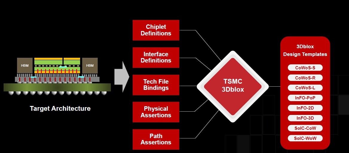
3Dblox 2.0 has won support from key EDA partners to develop design solutions that fully support all TSMC 3DFabric offerings. TSMC also launched the 3Dblox Committee, organized as an independent standard group, with the goal to create an industry-wide specification that enables system design with chiplets from any vendor. Working with members including Ansys, Cadence, Siemens, and Synopsys, the committee has technical groups that propose enhancements to the specs and maintain the interoperability of EDA tools. Designers can now download the latest 3Dblox specifications from the 3dblox.org website and find more information about 3Dblox and its tool implementation by EDA partners.

The Cadence Integrity 3D-IC platform fully supports the latest 3Dblox 2.0 std across all of TSMC’s 3D Fabric offerings including InFO, CoWoS and SoIC.
3D Fabric Alliance
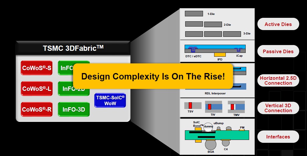
TSMC’s 3DFabric Alliance has been working toward the goal of providing customers with a full spectrum of proven solutions and services for semiconductor design, memory modules, substrate technology, testing, manufacturing, and packaging. The company now has 21 3DFabric Alliance partners across the industry.
TSMC has worked closely with Micron, Samsung Memory, and SK Hynix to drive rapid growth on HBM3 and HBM3e to advance generative AI systems by delivering more memory capacity.
TSMC has worked with substrate partners IBIDEN and UMTC to define a Substrate Design Tech file to facilitate substrate auto-routing.
TSMC is collaborating with automatic test equipment (ATE) partners Advantest and Teradyne on various 3D test challenges. To demonstrate high-speed test access for 3D stack testing through functional interface, TSMC is working with Synopsys and ATE partners on a silicon demonstrator to achieve the goal of 10x testing productivity boost. The Company is also working with all design-for-test (DFT) EDA partners to ensure effective and efficient interface testing.
For all the latest in Adv Pkging stay linked to IFTLE……………………………….