In the past 16 years, 3D InCites has watched the 3D packaging industry grow. The philosophy of 3D InCites was to create an advanced packaging community. At SEMICON West in Phoenix, the community was out in force, from ribbon-cutting ceremonies for new facilities, to new packaging equipment companies showing for the first time at SEMICON. At the show, I was able to interview parts of the community that are focused on advanced packaging. It was intriguing to see these many different players having unique solutions to move the future of advanced packaging forward. A shout-out to 3D InCites community member, Kiterocket, for arranging these interviews.
We will start with the process discussions and work our way up to 3D integration.
Leo Archer and Sally Ann Henry shared what ACM Research (ACMR) is doing in the 3D packaging space. ACMR made the transition to advanced packaging out of its front-end processes, as they commented, “the back end is the new front end”. The company has transitioned its equipment to handle the substrates used in advanced packaging, including panel-level packaging. One of the current challenges is that panel-level packaging and wafer-level packaging technologies are both being developed in parallel, so you need to be able to have solutions for both packaging technologies. To address this, ACMR has developed tools for electrochemical deposition and polishing, wafer clean, bevel clean, and vacuum clean for flux cleaning, which can accommodate both wafer-level processing and panel-level processing up to 600 by 600, and they are preparing for the 700 x 700 standards that are emerging.
VON ARDENNE develops thin film equipment, mostly for sputtering, but they have other applications as well. They have been working with Fraunhofer IZM to develop 3D packaging and other technologies for 3D packaging. Sven Frauenstein shared that they are very familiar with deposition on panels, which sets them up nicely for panel-level processing, as well as wafer-level processes. One of their systems has the capability of depositing film from both sides simultaneously. I could see this having some advantages for glass and silicon interposers, or bridges in deposition seed layers for vias. VON ARDENNE was highlighting its optical capabilities at SEMICON West with their OPTA X300 rotary disk coating system. The system was built specifically for electrical and optical layers. As optical interconnects become mainstream we could see this system gain some traction.
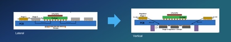
Power management is key to a well packaged system. As the packaging industry transitions from horizontal to vertical, power management is needed in the vertical direction. According to Eelco Bergman of Saras Micro Devices, having power management come in from the side on a 3D structure, there can be significant power loss and fluctuation as the current moves across the package. By placing the capacitors and inductors vertically in the substrate or PCB board, you can improve power loss and reduce the amount of heat generated in the package. You can also potentially lower processing costs as you are not depositing copper or silver across the PCB board; instead, you are attaching vertically to the substrate or PCB. Saras works with its vendors, substrate, and PCB suppliers to attach what it refers to as the Saras Tile, STILETM, vertically to the substrate. This helps to reduce the power needed and, more importantly, can reduce the heat generated, so less energy is needed to cool the system.
Metrology and testing will be a critical part of 3D implementation. New techniques will be needed to ensure that the packaged chips operate as designed and that the complex packaging process doesn’t have any defects.
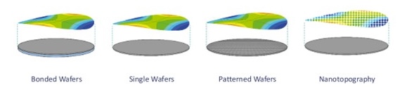
In my discussion with Jose Manuel, CEO and Founder of Wooptix. We discussed its Wave Front Phase Imaging, which is used to measure flatness on either a wafer or a panel. Called the Phemet lab tool, the system has an ultra-high resolution with 4700×4700 pixels. It can measure the entire wafer in one scan in under a second and provides sub-nanometer accuracy. From my perspective, this technology will be critical for the 3D packaging space, particularly in wafer and panel-level bonding. The WFPI tool can measure warpage and bow down to 1.2nm and is being used in DRAM manufacturing for uniformity, nanotopography, and roughness measurements. Having been around the industry for a bit, there are very few new process tools that pique my interest; this is one of them.

With 3D packaging and optical interconnects moving into the mainstream, testing these systems is critical to ensure that they work before you place them on the package and then before sealing the package up. Ira Leventhal of Advantest shared some of the challenges and the solutions they have developed to test the systems. As one can imagine, the 3D test landscape is very complex, and, as Ira put it, there are some very good test solutions out there, and others, as he phrased it, Ones that have been rushed to the test floor. To help address the test challenges, Advantest released its SiConic platform earlier in 2025, which creates a scalable ecosystem that empowers design verification and silicon validation teams within a unified, automated, and versatile environment. Advantest is also using AI to help develop test solutions. This is making good progress, but as with many AI solutions, it still needs engineering oversight. Advantest is also working with FormFactor on wafer-level testing solutions for silicon photonics chips using the V93000 SoC platform and with ficonTEC to develop a 300mm double-sided electro-optical wafer tester. This will hopefully speed the implementation of optical interconnects in the data centers and reduce power consumption.
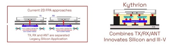
Circuits Integrated CEO Paolo Fioravanti and Chief Commercial Officer Carl McMahon shared how they are integrating III-V compound semiconductors and silicon in phased antenna arrays. They are employing 2.5D and 3D systems-in-package (SiPs) to integrate the transmit, receive, and antenna functions into a single 3D antenna-in-package/SiP architecture. This enables them to reduce flat panel antenna size, weight, power, and cost by more than 60%. In turn, this breakthrough enables faster, more sustainable, and agile SatCom networks for low Earth-orbit satellites, 5G, and defense applications. The picture below doesn’t really do the technology justice, as you are able to shrink the satellites to slightly larger than the size of a YETI 20 oz cup, which really demonstrates the power of heterogeneous integration and 3D packaging.
Rosie Medina, VP of Sales & Marketing for Promex, shared about the challenges of putting everything together. It all starts with early collaboration, and who is the right partner to create the integrated solution? Since most of the packaging projects Promex works on are not cookie-cutter it takes considerable coordination and education to make it work with items such as BGA substrates, material solutions, die stacking, and double-sided solutions, just to name a few. These are all areas that Promex must work with its customers to create the advanced package that will meet the customer’s solution. Advanced packaging has required Promex to dig a bit deeper and find out what the desired performance and outcomes are to develop the best packaging solution ecosystem for their customer. I’ve attached a link to a white paper that goes into how Promex addresses some of the challenges in their packaging and assembly process.
In summary, as ACMR put it, the back-end is the new front-end, and it’s giving the industry a lot of energy to push forward to that 1 trillion-dollar mark.