Overcoming yield loss, reliability risks, and scaling limits in advanced packaging with high-aspect-ratio copper interconnects.
As device architectures shrink, delivering high-reliability, fine-feature interconnects without sacrificing yield or performance has become a critical challenge for semiconductor manufacturers. In fan-out-wafer-level-packaging (FOWLP), chiplet-based designs, and high-density 2.5D/3D integration, the need for compact, high-performance interconnects is accelerating with the growth of high-performance computing (HPC) and artificial intelligence (AI) applications. The dual damascene process provides a proven solution, offering precise, scalable fabrication of high-aspect-ratio copper interconnects that meet the electrical, thermal, and mechanical demands of advanced wafer-level and 2.5D/3D packaging.
Originating in the back-end-of-line (BEOL) of semiconductor fabrication, the dual damascene process has evolved into a cornerstone of advanced packaging. Today, the dual damascene process is being applied to critical packaging structures such as redistribution layers (RDLs), silicon interposers, and hybrid bonding interfaces, in both wafer-level and panel-level packaging formats.
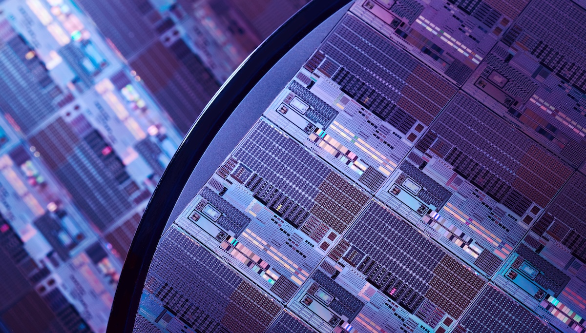
Unlike traditional subtractive methods that etch away deposited copper, dual damascene uses an additive copper metallization approach, filling etched vias and trenches with copper. This reduces material waste, improves process efficiency, and enables sub-2 µm line/space capability. These advances are vital for heterogeneous integration and 3D stacking, meeting the performance, power, and reliability requirements of today’s most advanced applications (Figure 1).
The Dual Damascene Process
Dual damascene is an additive copper metallization process that forms nanoscale vertical and horizontal features (vias and trenches) within a dielectric in a single metallization sequence. Instead of depositing a copper layer and patterning it through subtractive etching, dual damascene etches precise cavities into the dielectric, then fills them with copper via electroplating. This approach reduces material waste, improves process productivity, and scales efficiently to finer features.
In advanced packaging, where interconnect density, signal integrity, and thermal management are tightly linked, the dual damascene approach offers a compelling path forward. Its sub-2 µm line/space capability enables higher I/O density, while low-k dielectrics reduce parasitic capacitance. Shorter interconnect paths improve signal integrity, and tightly packed copper features with excellent coplanarity enhance thermal conduction, critical for high-power AI and HPC designs.
As feature sizes shrink, maintaining tight process control becomes critical. Precise via and trench alignment during etch, uniform deposition of diffusion barriers and seed layers, and high-quality chemical mechanical planarization (CMP) all directly influence yield and performance.
Key Process Steps:
- Dielectric deposition: Low-k or ultra-low-k dielectric materials are deposited to reduce parasitic capacitance between interconnects.
- Via and trench etching: Vias are etched first, followed by trenches, using advanced lithography and plasma etch techniques. These features are precisely aligned to enable stacked vertical and horizontal interconnects.
- Barrier and seed layer deposition: A diffusion barrier (e.g., TaN or Ru) is conformally deposited, followed by a thin copper seed layer by physical vapor deposition (PVD) to enable uniform electroplating.
- Copper electroplating: Both vias and trenches are filled with copper in a single plating step.
- CMP (chemical mechanical planarization): Excess copper is removed to produce a flat, inlaid surface, essential for multilayer stacking.
This sequence produces a tightly packed, low-resistance interconnect structure with excellent coplanarity, critical for heterogeneous integration and next-generation device scaling.
Why It Matters for Advanced Packaging
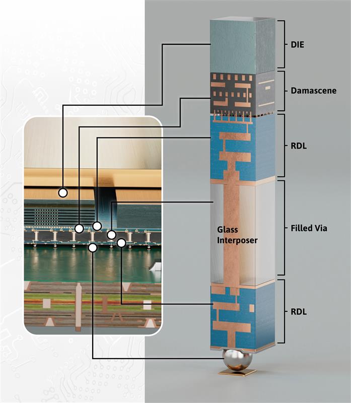
In advanced packaging, the dual damascene process supports performance, integration, and manufacturing requirements while enabling diverse chiplets to function seamlessly as one (Figure 2). It delivers:
- Higher I/O density: Shrinking line/space dimensions allow more interconnects per mm², ideal for FOWLP and silicon interposer designs.
- Improved signal integrity: Low-k dielectrics and shorter interconnect paths reduce resistive-capacitive (RC) delay, supporting the bandwidth and latency requirements in AI and HPC applications.
- Enhanced thermal performance: Dense copper networks improve heat dissipation in high-power chiplets and stacked devices.
- Process and cost efficiency: Combining via and trench fill into a single metallization step shortens processing time and reduces complexity. This is important for both wafer-level and panel-level scaling.
- Reliable multilayer integration: CMP achieves surface flatness across layers, enabling vertical stacking of redistribution layers (RDLs) and complex interconnect topologies.
- Compatibility with hybrid bonding and 3D stacking: CMP’s excellent surface planarity supports direct layer-to-layer bonding.
As line/space widths and pitches tighten and aspect ratios climb, the same process principles are now being adapted for 2 nm and angstrom-class logic nodes, driving fundamental changes to metallization materials and process flows.
Evolution of the Copper Damascene Roadmap: From 130 nm to 2 nm: The Road to Finer Pitches
For over two decades, the semiconductor industry has pursued an aggressive scaling trajectory. From the 130 nm nodes of the early 2000s to the imminent 2 nm era, each new technology node has brought finer line widths, narrower pitches, increased interconnect density, and higher via and trench aspect ratios. The introduction of fin field-effect transistors (FinFET) and gate-all-around (GAA) architecture has further intensified the complexity of routing and back-end-of-line (BEOL) metal stack integration. As a result, interconnect reliability, signal integrity, and process variability have emerged as critical factors impacting both yield and performance.
When widths and pitches drop below 20 nm, a host of new challenges emerge. The copper cross-sectional area decreases while barrier layers occupy a greater share of the interconnect volume, driving a steep rise in effective resistance. At the same time, capacitance increases as metal lines are packed more closely together, a problem that worsens with continued scaling. Filling these ultra-narrow, high-aspect-ratio trenches and vias also becomes increasingly difficult, with a higher risk of void formation during electroplating.
According to Yole Group, logic nodes below 5 nm are projected to account for over 20% of global wafer volume by 2027, with 2 nm entering full-scale production in 2025–2026. AI accelerators, HPC, and automotive semiconductors are pushing BEOL to its limits, driving the need for scalable, cost-effective interconnect solutions.
Meeting the Challenge: Seedless Copper Fill and Beyond
Traditional dual damascene uses conventional PVD to deposit a copper seed layer before electroplating. However, at sub-20 nm pitches and high-aspect-ratios, PVD struggles with conformality, resulting in gaps or thin spots in the seed layer. This non-uniform coverage makes it harder for electroplating to reliably fill the features, increasing the likelihood of voids and raising the risk of electromigration failure.
To address these challenges, the industry is advancing seedless copper electroplating techniques. Innovations include alternative barrier and seed materials such as ruthenium or cobalt, as well as copper plating directly onto the barrier layer itself. Regardless of the approach, the objective remains the same: to achieve reliable, void-free copper fill in narrow-pitch, high-aspect-ratio vias and trenches. This is critical for next-generation interconnect performance.
Industry Roadmaps and Implications for Damascene Interconnects
Leading semiconductor manufacturers, such as IBM, Intel, Rapidus, Samsung, and TSMC, are accelerating development toward 2 nm and angstrom-class nodes. This is driving fundamental changes in both transistor design and interconnect integration. These advanced nodes feature GAA transistors and will soon adopt backside power delivery (BPD), further increasing BEOL complexity.
BPD improves interconnect efficiency by relocating power lines to the wafer’s backside, allowing for wider, lower-resistance power routes. This separation of power and signal paths improves IR drop, reduces coupling, and enhances performance, while also allowing for greater logic density.
However, these innovations also introduce new BEOL challenges. As metal pitches shrink, GAA and BPD alter wiring layer geometries, and conventional PVD copper seed deposition struggles to maintain uniform coverage. To meet the tight dimensional tolerances and performance requirements of 2 nm and smaller nodes, the industry must develop new materials and process technologies that can reliably produce high-quality interconnects at these extreme scales.
BEOL, FEOL and the Evolving Role of Damascene Interconnects
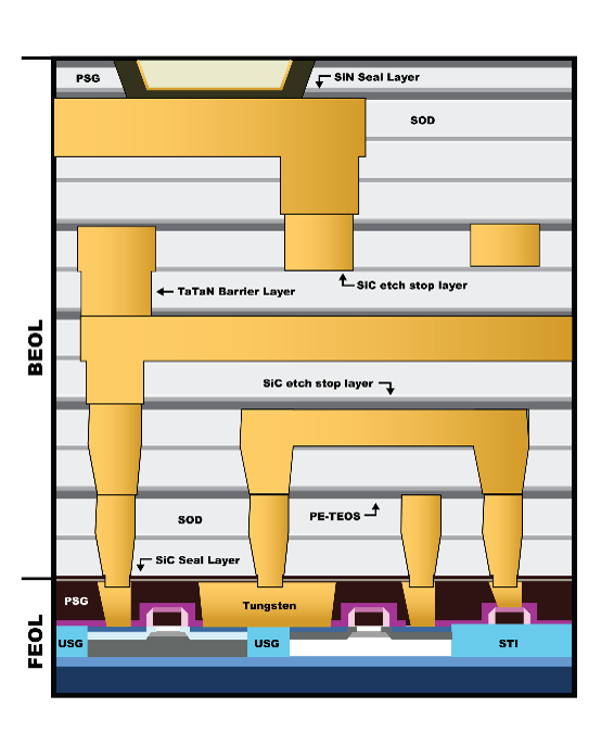
Semiconductor manufacturing is divided into two primary stages: front-end-of-line (FEOL) and back-end-of-line (BEOL) (Figure 3).
FEOL covers the formation of transistor and other active devices on the silicon wafer.

In traditional front-side power delivery networks (PDNs), both power and signals are routed through multiple BEOL metal layers. Near the transistor level, these layers become thinner and as line width and thickness shrink, electrical resistance increases, leading to greater voltage (IR) drops. This constrains routing flexibility and becomes an increasingly serious challenge at advanced nodes.
BEOL builds the interconnect stack using processes such as dielectric deposition, via/trench etching, copper metallization, and chemical mechanical planarization (CMP).
To overcome the scaling limits of front-side routing, a backside power delivery (BPD) approach is increasingly being adopted. By relocating the power grid to the wafer’s backside, where metal layers are wider and thicker, BPD enables lower-resistance power delivery. Freeing the front-side BEOL for signal routing only reduces congestion, improves signal integrity, and creates more room for interconnect scaling. The combined effect is reduced IR drop, enhanced performance, and greater logic density.
It is important to note that BPD relies on many damascene process steps, including CMP and copper fill, making it relevant to the evolution of interconnect technology. Industry leaders such as Intel, with its PowerVia approach, and TSMC are deploying BPD in high-performance devices. However, implementing BPD introduces new process challenges and thermal considerations, further underscoring the need for continued innovation in damascene interconnect technology.
Redefining Damascene for the Next Generation
At the 2 nm node and beyond, conventional damascene processes encounter significant challenges. PVD struggles to achieve uniform coverage as vias become deeper and narrower, leading to void formation, poor adhesion, and increased risk of electromigration. These issues intensify at high aspect ratios approaching 15:1, prompting fabricators to explore alternative metallization methods.
PVD also brings high capital equipment costs, extended cycle times, and significant maintenance demands, factors increasingly misaligned with aggressive production schedules and cost targets. After copper fill, achieving precise planarization with CMP becomes more complex as feature sizes shrink and topographies become more intricate.
A New Approach: Seedless Copper Deposition
To tackle these challenges, scientists at MacDermid Alpha developed a breakthrough alkaline based copper plating chemistry that eliminates the need for a PVD seed layer. This seedless approach deposits copper directly onto modern barrier liners, leveraging a precisely engineered synergy of three ligands that govern nucleation and fill dynamics.
By removing the PVD seed deposition step, the process streamlines the metallization workflow, removes a significant equipment bottleneck, and reduces cycle time. It enables void-free fill in high-aspect-ratio features, consistently delivering defect-free interconnects at production-relevant aspect ratios ranging from 2:1 to 5:1. The synergistic ligand system controls deposition behavior without the need for separate suppressor, accelerator, and leveler additives, simplifying chemistry management while improving process stability.
Beyond its technical advantages, the seedless approach offers a substantially lower cost of ownership compared to traditional PVD-plus-plating workflows. The ability to plate directly on the barrier layer while simultaneously filling vias enhances manufacturing efficiency, simplifies integration, and improves long-term reliability. This represents a paradigm shift in metallization, transitioning from multiple additive components to a unified ligand strategy delivering both simplicity and performance gains.
Materials Integration and CMP Compatibility
Part of the ViaForm® portfolio of copper damascene chemistries, this technology has been extensively validated for compatibility across key BEOL materials, including advanced barrier liners, low-k dielectrics, and CMP processes. It integrates seamlessly with modern metrology systems for real-time process monitoring and control and is supplied as a single-bath solution. Optional ligand feed systems allow straightforward adaptation to a wide range of plating platforms without major modifications, supporting both process flexibility and supply chain efficiency.
Ongoing Research and the Road Ahead
Collaborative research programs with leading foundries and universities are advancing both the understanding and the application of this seedless copper chemistry. Current studies focus on atomic-scale interactions between ligands and metal surfaces, predictive modelling of nucleation and growth behavior, and extending the approach to emerging architectures such as semi-damascene and subtractive metal patterning. These initiatives are strategically aligned with future technology node requirements, including sub-1.4 nm and angstrom-scale interconnects, ensuring the chemistry evolves in step with next-generation manufacturing challenges.
Unlocking Next Generation Interconnect Performance
As the semiconductor industry advances toward heterogeneous integration, high-density 2.5D/3D architectures, and the angstrom-scale era, interconnect technology is emerging as the defining factor in system performance. The dual damascene process, refined over decades in BEOL fabrication, has proven to be a scalable, precise, and cost-efficient method, ideally suited for advanced packaging. Its ability to form high-aspect-ratio copper interconnects with sub-2 µm line/space capability supports the I/O density, signal integrity, and thermal performance demanded by AI, HPC, and next-generation mobile applications.
Unlike subtractive approaches, dual damascene’s additive copper fill minimizes material waste, streamlines process flows, and achieves exceptional coplanarity, critical for multilayer RDL stacking, hybrid bonding, and chiplet integration. The integration of low-k dielectrics reduces parasitic capacitance, while shorter, denser copper paths improve both speed and power efficiency. Emerging innovations, such as seedless copper plating, build on these strengths by enabling reliable void-free fill in extreme aspect ratios while lowering cost of ownership.
By combining proven process maturity of a trusted process with cutting-edge adaptations, dual damascene remains at the center of the industry’s roadmap, enabling fine pitch interposers today and paving the way for backside power delivery (BPD) and sub-2 nm logic nodes of tomorrow. In short, it delivers the density, efficiency, and reliability that advanced packaging needs to keep pace with the relentless scaling and integration demands of next generation semiconductor devices.
MacDermid Alpha Electronics Solutions welcomes discussions with partners working to address the challenges of sub 2nm nodes and beyond.