
Challenges in the Era of Semiconductor Miniaturization
As process nodes continue to shrink, moving into the single-digit nanometer era, the challenges surrounding materials reliability and system performance are being redefined. With each new node, transistors become smaller enabling the integration of billions of transistors onto a single chip. However, this increased density also heightens sensitivity to the composition and quality of surrounding materials, including those used in packaging.
Advanced packaging architectures such as 2.5D and 3D ICs, now widely adopted in high-performance computing (HPC) and AI applications, amplify this sensitivity. These dense configurations create complex interactions between stacked and adjacent components, leading to tighter tolerances. This makes the materials increasingly sensitive to radiation-induced soft errors. One of the most overlooked contributors to these failures is alpha particle emissions from packaging materials, which can trigger soft errors (bit flips), single-event upsets, and system-level failures in data-sensitive applications.
The Silent Threat of Alpha Particle Emissions
Alpha particle emissions, once dismissed as inconsequential, has emerged as a critical reliability concern. Released by trace radioactive impurities in common materials like tin, these particles can strike sensitive areas of memory or logic, generating electron-hole pairs that lead to a temporary change in stored charge. The result can cause bit flips, inducing soft errors. In high-density devices like DRAM, SRAM, and AI processors, even a single error can lead to significant system-level consequences: corrupted data, system crashes, and degraded performance.
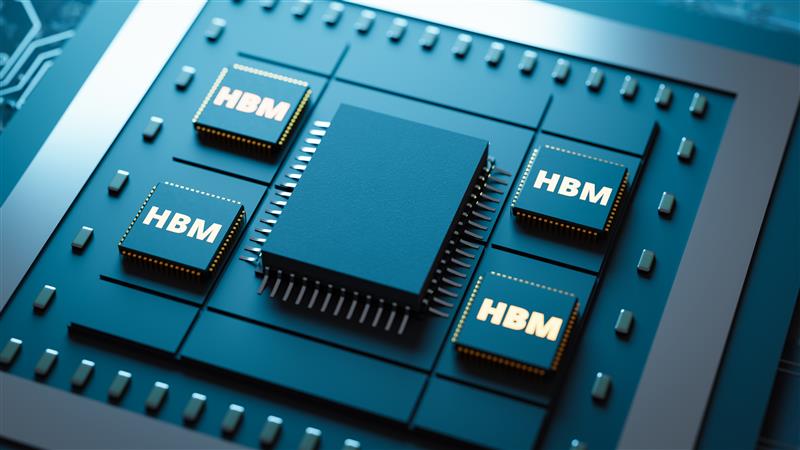
These effects are intensified in cutting-edge technologies like High-Bandwidth Memory (HBM) stacks, which are nearing data transfer rates of over 1 TB/s and are critical to AI workloads and HPC. The compact architectures and high interconnect densities of HBM stacks make them especially susceptible to radiation-induced soft errors. This highlights the importance of material purity throughout the entire package stack.
Shrinking Nodes, Growing Risk
As process nodes evolve from 7nm to 5nm and now toward 3nm and 2nm nodes, the energy required to store a bit continues to shrink. With these lower energy thresholds, there is virtually no margin for disturbances. Even minor energy disturbances such as alpha particle strikes can cause failures, triggering soft errors, and compromising performance and reliability.
Foundries across the industry, like TSMC, Intel, and Samsung are aggressively advancing ultra-fine pitch, high-density technologies to support the rising performance demands in AI, HPC, and advanced mobile applications (TrendForce, 2025). As manufacturing complexity increases, so does the challenge of maintaining yield and performance, making soft error mitigation a growing priority throughout the semiconductor supply chain, including material suppliers.
Market Forces Driving Change
Market analysts at Yole Group project rapid growth in HBM demand, citing its central role in AI and HPC applications. Their 2024 DRAM report delivers a clear message: soft error rates are becoming a major differentiator for packaging technologies. As a result, the need for ultra-low alpha materials is shifting from a best practice to a design mandate.
In response, foundries and OSATs (outsourced semiconductor assembly and test providers) are placing stricter requirements on material purity, especially for components used in advanced packaging. The industry is raising the bar on accepted material specifications, demanding low-emission materials. While once limited to aerospace and defense sectors, alpha emission specifications are now commonplace due to the rising importance of data integrity and system uptime.
Silent Failures: The Growing Risk of Alpha Emissions
In practical terms, soft errors caused by alpha emissions lead to silent data corruption, often going undetected until serious consequences arise. A 2020 study noted that large-scale Field Programmable Gate Array (FPGA) systems at high altitudes experienced one silent error every 3.75 hours across 100,000 nodes. Even rare errors can disrupt computations and corrupt data, leading to significant costs.
Low Alpha Plating Solutions: Extending Reliability at the Interconnect Level

Solder interconnects are close in proximity to sensitive circuits; as a result, they can be a significant source of alpha particle strikes. Given that these materials are applied in large volumes throughout a semiconductor package, their cumulative emission profile can become substantial. Consequently, demand for low alpha, ultra-low alpha (ULA) and even super-low alpha (SLA) solder alloys has grown.
Pure tin alloys, and more recently the transition to tin-silver alloys, have been fundamental materials for wafer-level packaging. However, as the semiconductor industry shifts toward more complex architectures like 2.5D and 3D, where interconnects are densely packed and vertically stacked, the potential impact of alpha emissions is amplified.
Standardization, Testing, and Engineering Strategies for Alpha Resilience
Industry standardization efforts accelerate the shift toward low alpha materials. The JEDEC JESD89A standard now defines methods for soft error rate (SER) characterization. While emerging IPC and IEC working groups are refining specifications for low alpha materials.
At the same time, advanced test methodologies, such as accelerated SER testing using neutron and alpha particle beams, are gaining traction in qualification labs. These tests simulate years of field operation within just a few days. This enables engineers to validate the alpha resilience of complete packages under realistic lab conditions.
Collaboration between academia, commercial labs, and industry groups is expanding data availability and improving the accuracy of SER prediction models. These tools enable engineers to assess the system-wide effects of materials early in the design phase, leading to more informed materials selection from the outset.

A Shift in Material Expectations
Addressing soft error reliability challenges requires materials engineered to reduce alpha particle emissions. This necessitates a fundamental shift in material sourcing practices. Sourcing high-quality raw materials, combined with process improvements designed to further enhance purity and control emissions, ensures materials meet the ever-increasing standards of the industry.
Our scientists tackled this challenge by developing an advanced purification process designed with tight control to deliver consistently high-quality, low alpha emission materials. Our low alpha solutions achieve alpha particle emission levels below 0.002 cts/khr-cm², which is well below industry standards.
To verify performance, every production batch undergoes alpha particle spectrometry, a highly sensitive method that quantifies emission rates with high confidence. Both purification and testing processes are fully traceable and designed to support the rigorous quality control demands of advanced semiconductor customers.
Low Alpha Tin Solutions
Low alpha tin solutions include both tin anodes and tin methanesulfonate (Sn-MSA) replenishers compatible with both soluble and insoluble anode plating systems. For systems using solid anodes, multiple form factors are available, including customer-specific geometries and pellets.
Flagship offerings include:
- MICROFAB® SN 002 A: A high-purity, stannous methane sulfonate designed for electroplating in semiconductor manufacturing. Available in low and ultra-low alpha variants.
- NOVAFAB® SN Pellets: High-purity (>99.99%) tin anodes in pellet form for use in soluble anode systems. Also available as customizable form factor anodes to meet specific plating requirements.
These low alpha tin materials offer plug-and-play compatibility with existing fab lines, delivering measurable gains in reliability by reducing the risk of alpha-induced soft errors.
Conclusion
As single-digit nanometer nodes and complex high-density stacked architectures become the standard in semiconductor technologies, alpha particle emissions have emerged as a critical reliability concern. Once dismissed as background noise, these emissions now pose serious threats to system integrity, particularly in memory-intensive and AI-driven applications.
With alpha particle-induced soft errors increasingly impacting performance, uptime, and data integrity, the adoption of ultra-low alpha materials must become a design requirement – on a par with electrical, thermal, and mechanical considerations.
MacDermid Alpha’s Low Alpha Tin portfolio offers a proven and advanced solution to this challenge. By applying rigorous in-house purification and alpha particle spectroscopy, these materials deliver measurable reductions in soft error risk. From MICROFAB SN 002 A, an acid-based replenisher to NOVAFAB SN Pellets for soluble anode configurations, we provide unmatched alpha suppression across a wide range of advanced semiconductor plating applications.
As chipmakers continue to push the boundaries of bandwidth, packaging density, and node scaling, one message is clear: alpha emissions must be controlled, not as a niche optimization but as a foundation for next-generation semiconductor reliability.
To learn more about low alpha plating solutions visit the MacDermid Alpha Electronics Solutions website.
References
- TSMC’s 3nm Capacity Hits 100,000 Wafers Next Year, Driven by New Projects, (2025) TrendForce